High-speed 850 nm vertical-cavity surface-emittinglasers with BCB planarization technique
2018-04-19 10:48:45HEXiaoyingDONGJianHUShuaiHEYanLVBenshunLUANXinxinLIChongHUZonghaiGUOXia
中國光學 2018年2期
HE Xiao-ying, DONG Jian , HU Shuai, HE Yan , LV Ben-shun, LUAN Xin-xin, LI Chong, HU Zong-hai, GUO Xia*
(1.School of Electronic Engineering,State Key Laboratory of Information Photonics andOptical Communications,Beijing University of Posts and Telecommunications,Beijing 100876,China; 2.School of Information, Beijing University of Technology,Beijing 100124,China)
1 Introduction
850 nm vertical-cavity surface-emitting lasers(VCSELs) are standard light sources for short-reached optical interconnects and data-communication links , including supercomputer clusters and data centers, because of their high modulation speed, low power consumption, low current operation, good beam quality, andetc.[1-3]. The modulation frequency of the VCSELs is mainly limited by their intrinsic resonance frequency, damping, and extrinsic parasitic parameters. Many methods were proposed to improve the modulation frequency of VCSELs, such as applying InGaAs/AlGaAs strain quantum wells to increase the differential gain and then the modulation frequency[4], optimizing the photon lifetime through etching top distributed Bragg reflector(DBR) to reduce the damping[5-6], and growing multiple oxide layers to decrease the oxide capacitance which is the largest parasitic capacitance in the devices[7-9].
In order to decrease the oxide capacitance, Benzocyclobutene(BCB), which is an important material for high-speed devices, is introduced into the VCSELs. Because it has a low dielectric constant of 2.65, lower to other frequently-used dielectric materials including SiO2and polyimide with dielectric constant of 3.9 and 3.3, respectively[10]. By planarizing the low-kBCB film between the P- and the N-type ohmic contact layer, the pad capacitance can be greatly reduced due to the capacitance calculation equation[11-12].
In this paper, high-speed oxide-confined 850 nm GaAs quantum wells(QWs) VCSELs using a low-kBCB planarization technique to reduce parasitic capacitance are reported. The small signal modulation bandwidths of the VCSEL with oxide aperture of 5 μm and 7 μm are demonstrated.
2 Design and Fabrication of High Speed VCSEL
The epitaxial structure of the VCSEL was grown by metal-organic chemical vapor deposition on a (100)-oriented n+-GaAs substrate. A graded separate confinement heterostructure region containing an active region with 3 unstrained 7 nm thick GaAs multiple quantum wells(MQWs) separated by 8 nm thick Al0.3Ga0.7As barriers was centered in the one-λresonant optical cavity with p-type and n-type Al0.3Ga0.7As phase compensation layers. The photoluminescence peak was located at 835 nm. 20.5 pairs of p-doped and 35 pairs of n-doped graded Al0.90Ga0.10As/Al0.12Ga0.88As DBRs were located on each side of the active region, respectively. A 30 nm thick Al0.98Ga0.02As layer, which was located near a node in the cavity standing wave profile where the optical intra-cavity scattering loss was reduced, was included in the top DBR to allow for selective oxidation during fabrication and then for transverse optical and electrical confinement. The topmost DBR layer consists of a 25 nm thick heavily p+-doped GaAs layer, located on top of the p-type DBR as a low-contact resistance layer.
Both the top and bottom mesa were fabricated by wet etching. The oxide aperture was formed in a wet oxidation furnace at 390 ℃ with an N2flow of 1 L/min, giving an oxidation rate of approximately 0.52 μm/min for the Al0.98Ga0.02As layers. An oxide aperture of 7 μm was selected. Ti/Au was sputtered on the top surface to form the ohmic contacts. Then, the devices were annealed in a rapid thermal annealing system at 430 ℃ in an N2atmosphere. Coplanar ground-signal-ground(GSG) contacts were applied for direct high-frequency probing measurements, in order to avoid parasitic coupling at the probe tips and thus improve the measurement accuracy of the microwave probing test[13].
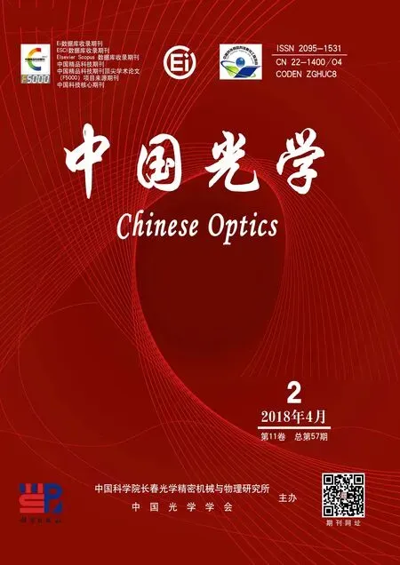
In this paper, the BCB is used to decrease the oxide capacitance of the VCSEL. Fig.1(a) shows the simulation results of the small signal modulation performance for the VCSELs with SiO2and BCB passivation, which comes from the small signal modulation transfer function derived by carrier and photon kinetic equations[14]. The parasitic cutoff frequency for VCSELs with the BCB passivation can reach to ~17.8 GHz, higher than that for SiO2-passivated ones about 10.6 GHz . Fig.1(b) demonstrated the small signal modulation response results measured by network analyzer, where the VCSELs are respectively passiated by SiO2and BCB both with the oxide aperture of 7 μm@6 mA. The -3 dB small signal modulation bandwidth is 15.2 GHz and 9.85 GHz, respectively, which indicates the modulation bandwidth limits by the RC parasitic parameter, thus to greatly increase its cutoff frequency depending on BCB passivation.
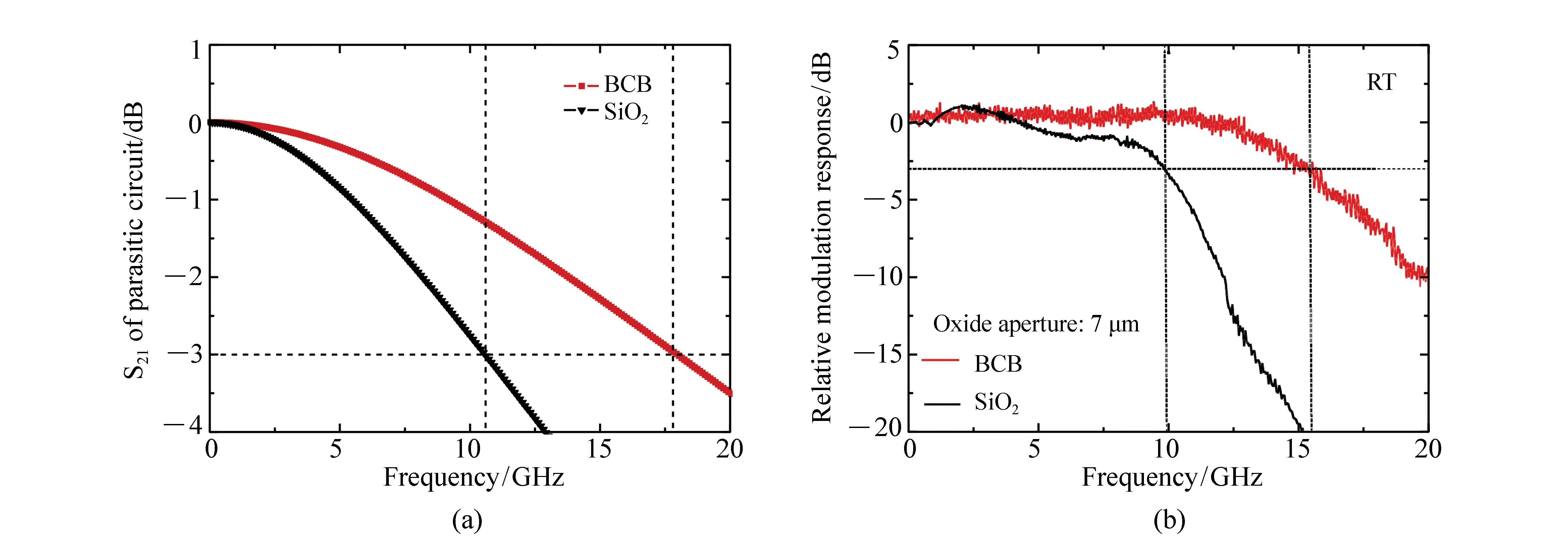
Fig.1 (a)Simulation results of small signal modulation response for VCSELs with BCB and SiO2 passivation. The parasitic cutoff frequency can reach to 17.8 GHz and 10.6 GHz for BCB and SiO2-passivated VCSEL, respectively. (b)The measured small signal modulation response for VCSELs with BCB and SiO2 passivation. The -3dB bandwidth is 15.2 GHz and 9.85 GHz with the oxide aperture of 7 μm@6 mA, respectively, which indicates the parasitic capacitance limits the modulation frequency of the devices
The schematic cross-sectional structure of high speed VCSEL devices is shown in Fig.2(a). Fig.2(b) presents a top-view image of the high-speed VCSEL.
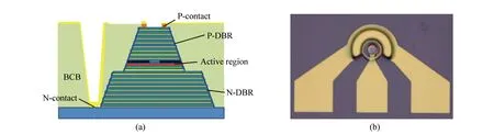
Fig.2 (a)Schematic cross-sectional structure of high-speed VCSEL devices. (b)Top-view image of the high-speed VCSEL with coplanar GSG electrode structure
The photosensitive BCB is coated on the VCSEL surface by spinning process. Fig.3(a) presents the dependence of the spinning speed on the BCB thickness before and after hard baking of 1.5 min with the temperature of 70 ℃ in the oven. According to the epitaxial structure, the spinning speed is selected to be 2 000 r/min with the BCB thickness of around 6 μm. The thick film requires more exposure energy. Fig.3(b) shows the relationship of exposure time with the diameter difference(Δd) between patterns on the mask and on the devices. Generally, the pattern size on the devices is larger than that on the mask. The diameter difference increases with the exposure time because the diffraction occurs at the edge of the mask patterns. Decreasing the exposure time will decrease the pattern size discrepancy, however, and the residues on the patterns are hard to be removed due to the thick BCB film determined by the VCSEL structure. Fig.3(c) demonstrates the microscopic image of the exposed area. Colorful strips are caused by the refractive index difference between the residue BCB and the substrate, which will deteriorate the Ohmic contact. In our experiment, inductively coupled plasma(ICP) etching with SF6and O2chemistry is applied to remove these BCB residues. Fig.3(d) demonstrates the microscopic image of the pattern after the ICP etching using SF6/O2chemistry with ICP power of 1 000 W and RF power of 50 W.
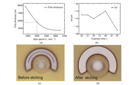
Fig.3 (a)Relationship between spin speed and film thickness of BCB. (b)Difference in aperture diameter(Δd) between lithography and BCB patterns at various exposure times. (c)Top-view images of the thin BCB layer before dry etching and (d)after dry etching
3 Static and Dynamic Performance Characteristics
The static light output power-current-voltage(L-I-V) characteristics were measured under the wafer probes at room temperature. The L-I-V results for BCB planarization VCSELs with the 5 μm and 7 μm oxide aperture diameter are shown in Fig.4(a). It can be seen that the threshold currentsIthare 0.12 mA and 0.22 mA, and the threshold electrical powers are 0.65 mW and 0.84 mW at the 5 μm and 7 μm oxide aperture, respectively[15], while the threshold current densityJthis about 0.57 kA/cm2. As the current injection increases, the photon density in the active region increases and the optical power also increases. Correspondingly, the maximum output optical power increased with aperture size. The maximum output optical power reached to 0.47 mW at a 9 mA and 0.68 mW at a 12 mA respectively for the 5 μm and 7 μm oxide aperture VCSELs. That is because red shift in wavelength and decrease in efficiency would be caused by self-heating effects, and optical power therefore decreased rapidly. The differential resistance, depending on the size of the oxide aperture and epitaxial structure[16], are 212 Ω and 190 Ω at the 5 μm and 7 μm oxide aperture, which determines the thermal roll-over current of the VCSELs.
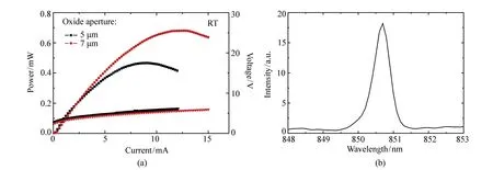
Fig.4 (a)Static P-I-V characteristics of BCB-planarized VCSELs with a 5 μm and 7 μm oxide aperture at room temperature. (b)Electrical-luminescence spectrum for the VCSEL at room temperature and current injection of 10.0 mA
The small signal modulation response of the VCSELs was measured using a 40 GHz R&S ZVA 40 network analyzer and a high-frequency microwave probe(Picoprobe 40A-GSG-150-P) to contact the device under test. A multimode fiber was connected to a 25 GHz high-speed photodetector(New Focus 1414-50), and the signal after detection was connected back to the network analyzer with a high-frequency cable. Before testing the VCSELs, calibrations were made to compensate for losses caused by the cables and the probe insertion[17]. Fig.5 show small-signal modulation response at room temperature at different bias currents for the 5 μm(a) and 7 μm(b) oxide aperture VCSELs with BCB planarization. For the 5 μm oxide aperture VCSEL, as the injection current increases from 2 mA to 5 mA, the small signal modulation bandwidth increases from 12.8 GHz to the maximum 15 GHz due to increased gain. Then the modulation bandwidth decreased to 14.3 GHz at 8 mA injection current due to heat generation inside the device. For the 7 μm oxide aperture VCSEL, as the injection current increases from 3 mA to 9 mA, the small signal modulation bandwidth increases from 14.1 GHz to the maximum 15.2 GHz, and then dropped to 13.1 GHz. Under small injection current bias at 2 mA for 5 μm oxide aperture and 3 mA for 7 μm oxide aperture, the intensity modulation can follow the current modulation up to resonance frequency. An obvious enhancement of modulation response exists at the resonance. As shown in Fig.5, beyond the resonance, the response dropped off dramatically. While, under the large injection currents, the responses measured in Fig.5 are flat without peak frequency of resonance. The -3 dB modulation bandwidth increases with the resonance frequency until the damping becomes more and more strong. At same time, the -3 dB modulation bandwidth decreases with the further increase of resonance frequency and the damping.
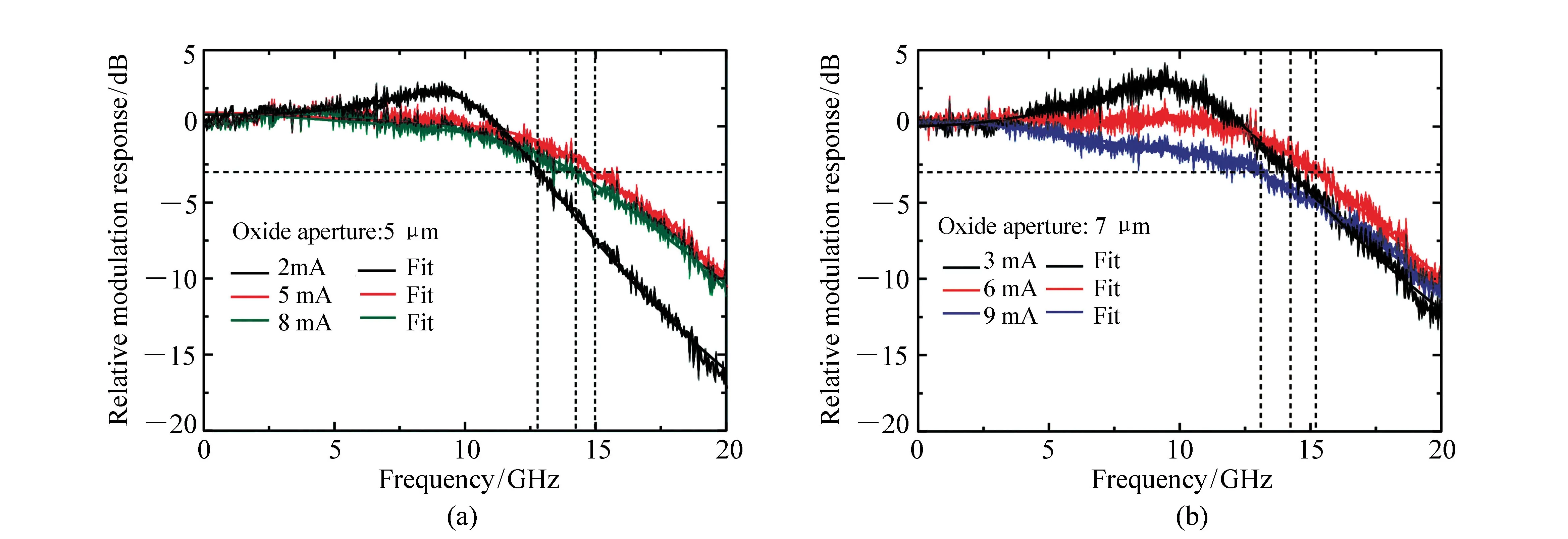
Fig.5 Small-signal modulation response at room temperature at different bias currents for the BCB-planarized VCSEL with (a)5 μm and (b)7 μm oxide aperture
Fig.6(a) plots the resonance frequency depending on the square value of injection current above the threshold currentIthfor the VCSEL with oxide aperture of 5 μm and 7 μm. The data of resonance frequency is extracted from the fitting of the curves in Fig.5 according to the transfer function[18]. As show in Fig.6(a), resonance frequencyfrincreases linearly with the low injection current. The slope, which is the rate of the resonance frequency increased with bias current, could be defined as D-factor of 8.746 GHz/mA1/2and 7.492 GHz/mA1/2, for 5 μm and 7 μm oxide aperture VCSELs, respectively. The reason is that, under the same injection current, VCSEL with small oxide aperture has a smaller active region volume than that of lager oxide aperture.
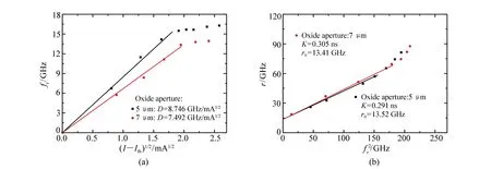
Fig.6 (a)Plot of the resonance frequency for the VCSELs with 5 μm and 7 μm oxide aperture versus the square root of the current injection above the threshold current at room temperature. (b)Damping rate versus resonance frequency square for the VCSELs with 5 μm and 7 μm oxide aperture at room temperature
Fig.6(b) plots the dependence of damping on the square of resonance frequency for the VCSELs with the oxide aperture of 5 μm and 7 μm, respectively. All the damping data are also extracted from the fitting results for the curves in Fig.5. The damping increases in proportion to resonance frequency, which can be described as follows[19]
(1)

4 Conclusion
High-speed oxide confined 850 nm GaAs QWs VCSELs were designed and fabricated using a low-kBCB planarization technique. BCB has a very low dielectric constant of 2.65 and a 6 μm thick layer was deposited using a spin-coating process. The parasitic cutoff frequency of the VCSEL using BCB planarization technique increased from 10.6 GHz to 17.8 GHz compared with the SiO2-passivated VCSEL at 7 μm oxide aperture. The small signal modulation bandwidth of the low-kBCB planarization VCSELs with 5 μm and 7 μm oxide aperture have been achieved to 15 GHz and 15.2 GHz, respectively, mainly limited by the damping and resonance frequency.
[1]海一娜,鄒永剛,田錕,等.水平腔面發射半導體激光器研究進展[J].中國光學,2017,10(2):194-206.
HAI Y N,ZOU Y G,TIAN K,etal. Research progress of horizontal cavity surface emitting semiconductor lasers[J].ChineseOptics,2017,10(2):194-206.
[2]黃海華,劉云,楊曄,等.850 nm錐形半導體激光器的溫度特性[J].中國光學,2013,6(2):201-207.
HAI H H,LIU Y,YANG Y,etal. Temperature characteristics of 850 nm tapered semiconductor lasers[J].ChineseOptics,2013,6(2):201-207.
[3]戚曉東,葉淑娟,張楠,等.面發射分布反饋半導體激光器及光柵耦合半導體激光器[J].中國光學,2010,3(5):415-431.
QI X D,YE SH J,ZHANG N,etal. Surface-emitting distributed-feedback semiconductor lasers and grating-coupled laser diodes[J].ChineseOptics,2010,3(5):415-431.
[4]WESTBERGH P,GUSTAVSSON J S,HAGLUND A,etal.. High-speed, low-current-density 850 nm VCSELs[J].IEEEJ.Sel.TopicsQuantumElectron.,2009,15(3):694-703.
[5]WESTBERGH P,GUSTAVSSON J S,KO?GEL B,etal.. Impact of photon lifetime on high-speed VCSEL performance[J].IEEEJ.Sel.TopicsQuantumElectron.,2011,17(6):1603-1613.
[6]LARISCH G,MOSER P,LOTT J A,etal.. Impact of photon lifetime on the temperature stability of 50 Gb/s 980 nm VCSELs[J].IEEEPhoton.Technol.Lett.,2016,28(21):2327-2330.
[7]HAGLUND E,WESTBERGH P,GUSTAVSSON J S,etal.. High-speed VCSELs with strong confinement of optical fields and carriers[J].J.LightwaveTechnol.,2016,34(2):269-277.
[8]MOSER P,LOTT J A,BIMBERG D. Energy efficiency of directly modulated oxide-confined high bit rate 850-nm VCSELs for optical interconnects[J].IEEEJ.Sel.TopicsQuantumElectron.,2013,19(4):1702212-1702212.
[9]WESTBERGH P,SAFAISINI R,HAGLUND E,etal.. High-speed oxide confined 850-nm VCSELs operating error-free at 40 Gb/s up to 85 ℃[J].IEEEPhoton.Technol.Lett.,2013,25(8):768-771.
[10]LUCOVSKY G,RAYNER JR G B. Microscopic model for enhanced dielectric constants in low concentration SiO2-rich noncrystalline Zr and Hf silicate alloys[J].Appl.Phys.Lett.,2000,77(18):2912-2914.
[11]OU Y,GUSTAVSSON J S,WESTBERGH P,etal.. Impedance characteristics and parasitic speed limitations of high-speed 850-nm VCSELs[J].IEEEPhoton.Technol.Lett.,2009,21(24):1840-1842.
[12]CHANG Y C,COLDREN L A. Efficient, high-data-rate, tapered oxide-aperture vertical-cavity surface-emitting lasers[J].IEEEJ.Sel.TopicsQuantumElectron.,2009,15(3):704-715.
[13]LI H,LOTT J A,WOLF P,etal.. Temperature-dependent impedance characteristics of temperature-stable high-speed 980-nm VCSELs[J].IEEEPhoton.Technol.Lett.,2015,27(8):832-835.
[14]COLDREN L A,CORZINE S W,MASHANOVITCH M L.DiodeLasersandPhotonicIntegratedCircuits[M]. New Jersey,MD:John Wiley & Sons,2012.
[15]LI H,WOLF P,MOSER P,etal.. Impact of the quantum well gain-to-cavity etalon wavelength offset on the high temperature performance of high bit rate 980-nm VCSELs[J].IEEEJ.QuantumElectron.,2014,50(8):613-621.
[16]MOSER P,LOTT J A,LARISCH G,etal.. Impact of the oxide-aperture diameter on the energy efficiency, bandwidth, and temperature stability of 980-nm VCSELs[J].J.LightwaveTechnol.,2015,33(4):825-831.
[17]LARSSON A,WESTBERGH P,GUSTAVSSON J,etal.. High-speed VCSELs for short reach communication[J].Semicond.Sci.Technol.,2010,26(1):014017.
[18]HAGLUND E P,KUMARI S,WESTBERGH P,etal.. 20-Gb/s modulation of silicon-integrated short-wavelength hybrid-cavity VCSELs[J].IEEEPhoton.Technol.Lett.,2016,28(8):856-859.
[19]HAGLUND E P,WESTBERGH P,GUSTAVSSON J S,etal.. Impact of damping on high-speed large signal VCSEL dynamics[J].J.LightwaveTechnol,2015,33(4):795-801.