Design of a Silicon-Based High-Speed Plasmonic Modulator
2012-05-21 03:41:00MuXuJiayangWuTaoWangandYikaiSu
ZTE Communications 2012年1期
Mu Xu,Jiayang Wu,Tao Wang,and Yikai Su
(State Key Laboratory of Advanced Optical Communication Systems and Networks,ShanghaiJiaotong University,Shanghai200240,P.R.China)
Abstract In this paper,we propose a silicon-based high-speed plasmonic modulator.The modulator has a double-layer structure with a 16μm long metal-dielectric-metal plasmonic waveguide at the upper layer and two silicon single-mode waveguides at the bottom layer.The upper-layer plasmonic waveguide acts as a phase shifter and has a dielectric slot that is 30 nm wide.Two taper structures that have gradually varied widths are introduced at the bottom layer to convert the photonic mode into plasmonic-slot mode with improved coupling efficiency.For a modulator with two 1μm-long mode couplers,simulation shows that there is an insertion loss of less than 11 d B and a half-wave voltage of 3.65 V.The modulation bandwidth of the proposed modulator can be more than 100 GHz without the carrier effect being a limiting factor in silicon.The fabrication process is also discussed,and the proposed design is shown to be feasible with a hybrid of CMOSand polymer technology.
Keyw ords plasmonic phase modulator;gradually varied taper;high speed
1 Introduction
A modulator is a critically important device in optical communication systems and short-reach electro-opticalinterconnects.Modulation speed continues to improve and is now well above 100 GHz,which rivals the processing speed of state-of-the-art CMOSelectronic devices.The silicon optical modulators described in this paper are capable of having a modulation bandwidth of more than 40 GHz[1],depending on whether carrier accumulation[2],carrier injection[3],or carrier depletion[4]is used.
To enable carrier accumulation in silicon,a metal-oxide semiconductor(MOS)structure is preferred.In such a structure,the metal acts as the electrode,and the oxide acts as the barrier.When voltage is applied,free carriers accumulate at the interface between the oxide and the semiconductor.In 2004,A.Liu et al.fabricated the first silicon-based carrier accumulation modulator[2].Although the device only had 1 GHz bandwidth,it paved the way for future silicon modulators.
Carrier injection can be achieved by using a forward-biased silicon P-I-Ndiode,and depletion can be achieved by using a reverse-biased silicon P-N diode.In 2007,Q.Xu et al.fabricated a silicon-ring-based carrier-injection modulator with a bandwidth of more than 12.5 GHz[3].In 2008,S.J.Spector et al.increased the bandwidth of a silicon-based carrier-injection modulator to more than 26 GHz,even reaching up to 40 GHz[1].In 2010,Po Dong et al.used silicon carrier-depletion modulators integrated on 0.25μm long silicon-on-insulator(SOI)waveguides with VπLof 1.4 V-cm to show that low energy consumption in a silicon modulator is feasible[4].
One of the limitations of silicon is two-photon absorption(TPA),which makes it hard to further increase modulation bandwidth[5].To overcome this limitation,a silicon-organic hybrid(SOH)approach has been suggested.By combining silicon waveguides with highly nonlinear electro-optical(EO)organic materials or high-absorption multilayer III-V Quantum well materials,the modulation speed can be increased to more than 30 GHz[6],[7].In 2011,L.Alloattiet al.developed an SOH-platform-based electro-optic modulator that operated at 42.7 Gb/s and had a VπL of about 9 V-mm[6].
Although the response speed of x(2)nonlinearity in organic material can be at least 165 GHz[8],the speed of the practical modulator is still limited because of the weak confinement,which causes a considerable proportion of light to leak into the transparent silicon electrodes.Recent progress in plasmonic silicon photonics has greatly improved confinement in the waveguides,and this is promising for the design of future ultracompact photonic devices.However,although confinement is improved,optical loss increases because of Ohmic loss in the metal and scattering at the grain boundaries[9].These prevent plasmonic devices from many long-range and large-scale applications.Several silicon-based modulators with plasmonic waveguides have been theoretically described[10],[11].In 2011,S.Zhu et al.fabricated a metal insulator silicon-based plasmonic modulator[12].The modulator was 4μm long and included two couplers.Although they are compact,the schemes in[10]-[12]have large loss and low modulation efficiency.
2 Device Structure and Mode Confinement
The structure of the phase modulator comprises two layers.The bottom layer comprises two unconnected silicon waveguides coated with silicon oxide for converting between photonic mode and plasmonic mode(Fig.1).The waveguides have cross-sections of 400×220 nm2.The upper layer mainly comprises two parallel symmetric metal plates made from,for example,silver,and coated with an EO polymer to form an MDM structure.The polymer fills a 30 nm wide gap.The metal plates are 16μm long and 100 nm wide and extend to both sides in order to enable electrodes to contact.The overlap between the bottom silicon waveguides and the upper metal plates ranges in length from 1 to 1.5μm and is mainly determined by the coupling length between the different modes supported by silicon and MDM waveguides.Two gradually varied tapers are introduced at the overlapping area of the silicon waveguides in order to enhance coupling efficiency.The proposed width of the taper’s end face is 400 nm,and the proposed width of the taper’s head face is 300 nm.
The phase modulator uses the Pockels effect of a nonlinear polymer to produce refractive index variation and phase shift.With an appropriate synthesis and poling process,there is great potential for the nonlinear EO to have a high EO coefficient[13],large dynamic refracitve index range[14],and greater resistance relative to other material fabrication processes[15].However,in most EO-polymer-based SOH modulators,the confinement capability of the dielectric waveguides is limited,and modulation efficiency is greatly reduced by the mode energy leaking from the polymer area into the silicon waveguides.Nevertheless,plasmonic waveguides such as conductor-gap dielectric(CGD)and MDM may be a promising solution to improving mode confinement of the polymer area and increasing the refractive index tuning efficiency.Fig.2 shows the contrast between the electric field intensity profiles of the MDM-slot waveguide and the silicon-slot waveguide that is coated with a polymer with refractive index of 1.63.The height of the plasmonic-slot waveguide is 100 nm,and the width of the slot is 30 nm.The height of the silicon-slot waveguide is 220 nm,and the width of the slot is 30 nm.Using the finite-difference time-domain(FDTD)method,we calculate the electric field energy within the slot regions defined by the white dotted lines in Fig.2.In the plasmonic-slot waveguide in Fig.2(a),69.335%of the electric-field energy is confined within the slot.In the silicon-slot waveguide,shown in Fig.2(b),27.956%of the electric field energy is confined within the slot because of considerable leakage of the mode into the silicon slab.With a larger proportion of the light accumulated in the slot region,modulation can be improved by a factor of two.
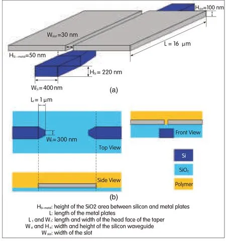
▲Figure 1.Structure of the silicon-based plasmonic phase modulator:(a)overall perspective of the phase modulator without coatingmaterials,(b)top view of the bottom layer,side and front view of thephase modulator.
3 Key Technologies for a High-Speed Plasmonic Phase Modulator
3.1 Phase Modulation and High-Speed Characteristic
After efficient poling[16],the EO polymer has a high EO coefficient of 100-200 pm/V.The proposed device uses AJLS103 EO polymer cross-linked with polymethyl methacrylate(PMMA)[15]with a refractive index,ne,of approximately 1.63 and an EO coefficient,γ33,of approximately 150 pm/Vat 1550 nm wavelength.Nonlinear EO polymers typically have a very high resistivity of more than 1011Ω·cm[17],so the two parallel metal plates comprising the slot are electrically isolated and can be used as the modulator electrodes.Then,the refractive index variance of the polymer under applied voltage can be expressed as
where V is the applied voltage and d is the slot width.The phase shift induced by the refractive index variance can be expressed as

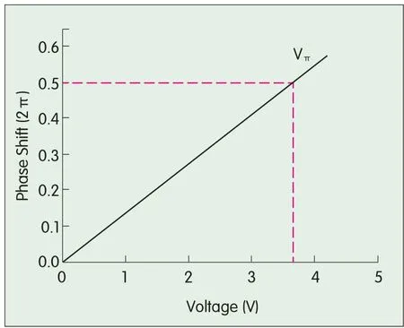
where l is the effective modulation length andГis the proportion of the electric field energy inside the polymer slot.Phase modulation can be plotted against voltage for l=14μm,d=30 nm,andГ=70%,and the half-wave voltage Vπ=3.652 Vcan be read from the curve at phase shiftπ(Fig.3).In(1),the maximum refractive index variance is 0.0392,and this is achievable using the proposed high-nonlinear EO polymer[14],[18].The loss in the plasmonic MDM-slot waveguide is 0.38 d B/μm and is calculated using FDTDsimulation.The loss in the phase shifter is 0.38×l,where l=5.32 d B.The half-wave voltage-length product can be as small as 0.0051 cm·Vwith Vπ=3.652 V.Aphase-shifter loss of 5.32 d B is tolerable.The intersection of the red dotted lines in Fig.3 is the value of the half-wave voltage that leads to aπphase shift.
One of the attractive features of the plasmonic phase modulator is its potential for high modulation speed because it is compact and has strong optical confinement in the slot.In the proposed design,the polymer can be treated as an insulator.Fig.4 shows the schematic of the plasmonic-slot waveguide.The two parallel metal plates with sandwiched EO polymer form a capacitor.The anode and cathode are fabricated over the extended silver plates to enable electrical signal input.From C=ε0εγA/d,the capacity is nearly on the order of severalfF.The permittivity of the vacuum isε0;the dielectric constant of 2.657 isεγthe lateral area of the metal plates is A;and the thickness of the metal plates is d.The modulation bandwidth,fmax,is proportional to 1/RC,where R is the external loading resistance(R=50Ωin plasmonic modulator designs)[19].The modulation bandwidth can be on the order of terahertz,which exceeds the processing bandwidth of state-of-the-art electronic CMOSdevices.In plasmonic modulators,the metal parts can be used as electrodes to conduct signal voltage directly to the active material.This is unlike silicon photonic modulators,which rely on free carriers in the semiconductor to transport electrical signals.Thus,the timeτneeded for the free-carrier transport process can be significantly reduced,and this greatly increases the response speed of the model shown in Fig.4.
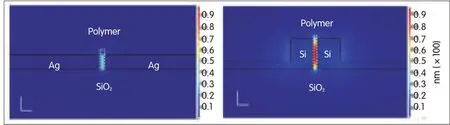
▲Figure 2.Electric field-intensity mode profiles of(a)plasmonic-slot waveguide and(b)silicon-slotwaveguide.The intersecting lines(bottom left)indicate a scale of 100 nm.
3.2 Photonic to Plasmonic Mode Conversion
Because of the internal loss mechanism of metal towards light at the wavelength of 1550 nm,plasmonic slot waveguides have larger optical loss compared with silicon waveguides,and this prevents plasma waves from being used in far-reach and large-scale applications[20].Couplers used for converting photonic and plasmonic modes rely on silicon waveguides as the optical transmission medium and are very important.We propose a gradually varied taper for conversion in the plasmonic phase modulator.The taper overlaps underneath the plasmonic-slot waveguide with longitude of about 1μm.The width of the taper’s end face is 400 nm,and the width of the taper’s head face is 300 nm.
To achieve high coupling efficiency between the photonic and plasmonic modes,correctly configuring the overlap between the upper plasmonic waveguide and bottom silicon waveguides is critical.Here,we analyze the cross-section in the overlapping area with the upper and bottom waveguides in Fig.5.There is an efficient coupling process in the two-layer parallel waveguides structure[21];thus,from coupling mode theory,we can assume that even modes and odd modes appear coincidently within the proposed double-layer distribution[22].The coupling between the photonic and plasmonic modes can be modeled as a process of the modes’propagation and interference.The coupling length,lc,is given by

whereβеandβоare the corresponding optical propagation constants of the even modes and odd modes,respectively.The maximum optical power coupled from one waveguide tothe other is modeled in[21]and given by
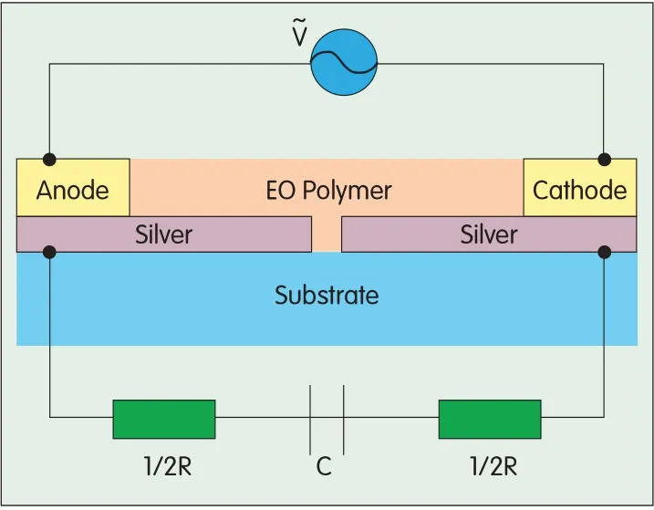
Figure 4.?The electrical characteristic modelof the proposed phase modulator.
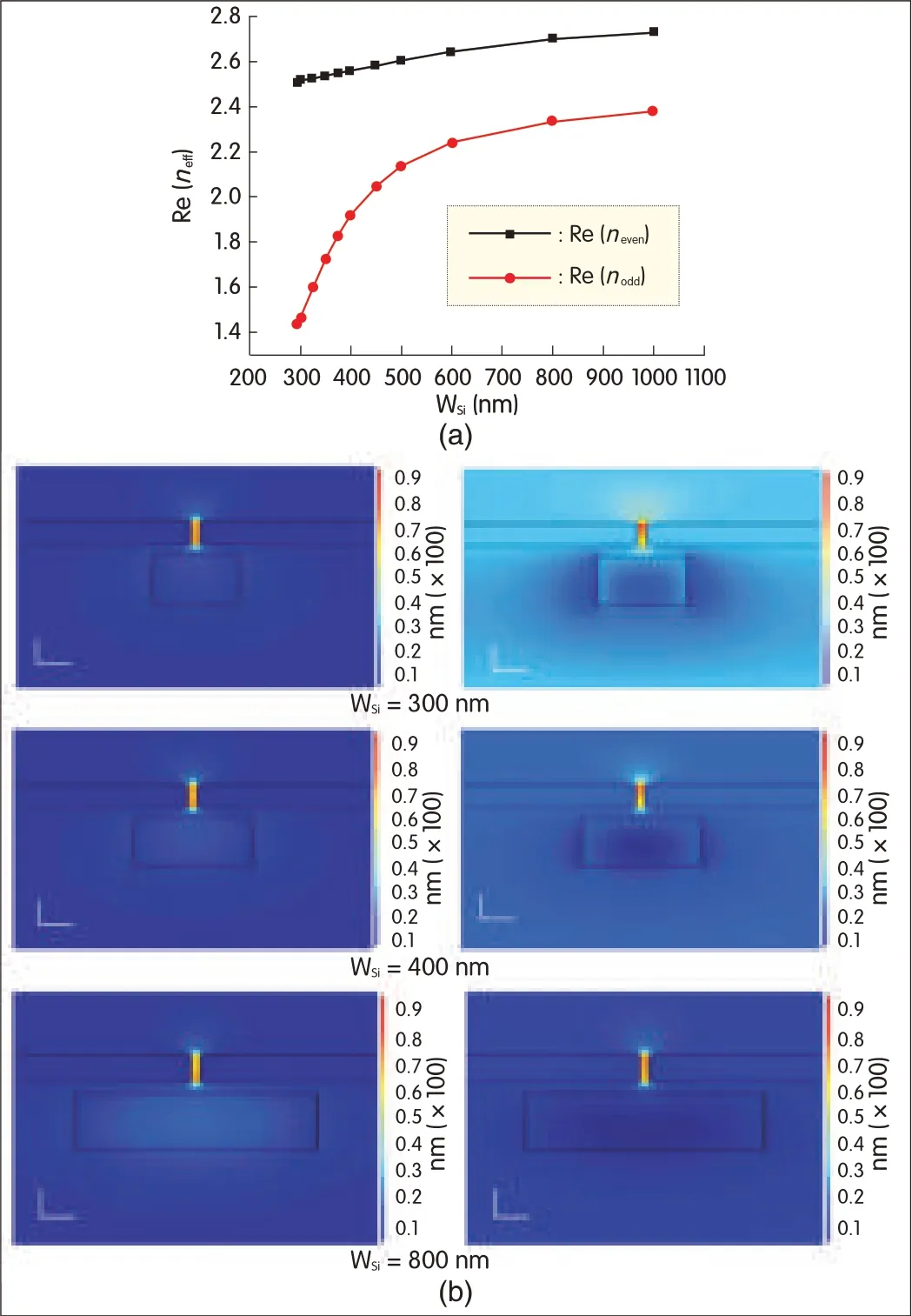
▲Figure 5.(a)Effective refraction index of even and odd modes versus Wsi in the proposed double-layer waveguide profile,(b)Ex componentintensity of the even(left)and odd(right)TEmodes at Wsi of 300 nm,400 nm,and 800 nm.

where x=2lc/πl(wèi)p,and lpis the average attenuation length of the lossy waveguides.From(4),given the loss coefficient of the waveguides,higher maximum transferring optical power can be achieved with shorter coupling.Fig.5(a)shows the contrast between the effective refraction index of the even and odd modes in the profile of the proposed double-layer waveguides.Fig.5(b)shows the electric field-intensities,Ex,of the two modes at silicon waveguide widths of 300 nm,400 nm,and 800 nm.The horizontals in the 90°angles(bottome left)are a scale of 100 nm,and the verticals are a scale of 100 nm.These electric field intensities are obtained using FDTD.Both even and odd modes are transverse electric(TE)modes and are dominant inside the plasmonic-slot waveguide.As the width of the silicon waveguide becomes narrower,the difference between the effective refraction index of the two modes becomes larger,leading to a shorter coupling length(Fig.6).Thus,from(4),a larger fraction of power coupling from one waveguide to another is also achieved.Reducing the width of the silicon waveguide can improve coupling efficiency.However,if the dimensions of the silicon waveguide are too small,the magnetic field is less confined within the core and a larger proportion of Poynting vector leaks into the cladding.Thus,the mode of the optical field is cut off.In waveguide optics,such a process can be quantified as a normalized propagation constant[23]:

where neffis the effective refraction index of the optical mode,and ncladand ncoreare the refraction indexes of the cladding and core area within the waveguides.If B≤0,the effective refraction index of the particular mode is less than that of the cladding,and the mode is cut off[23].The B curve for the proposed waveguides at the overlapping area is plotted in Fig.7.When the width of the silicon waveguide is less than 295 nm,the normalized propagation constant of the TEodd mode is less than zero,and the mode is cut off.Therefore,the proposed couplers use two tapers with widths that gradually vary from 400 nm at the end face to 300 nm at the head face.These tapers reduce the coupling length to the greatest possible extent,and the TEodd mode is not cut off.
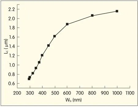
Figure 6.?Coupling length versus Wsi.
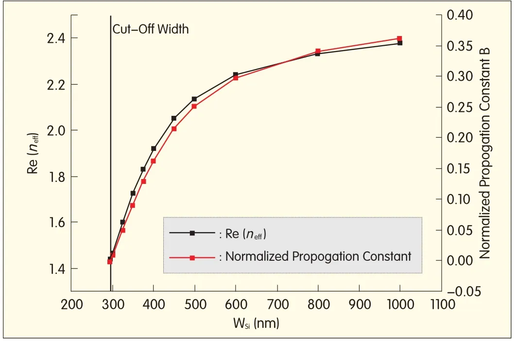
▲Figure 7.Effective refraction index and normalized propagation constant of photonic mode versus Wsi.
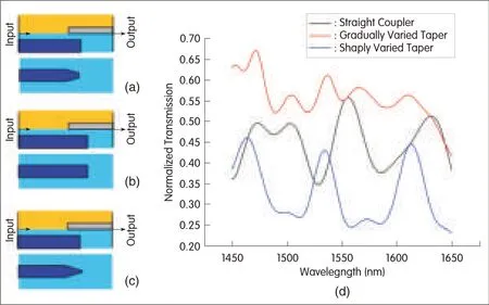
▲Figure 8.Coupling efficiency for(a)the proposed taper with a width that gradually changes from 400 nm to 300 nm,(b)straightwaveguide withouttaper,and(c)taper with a width that changes sharply from 400 nm to 80 nm.d)Outputtransmission for the three coupling structures.
Three-dimensional simulations of coupling efficiency are performed using FDTD(Fig.8).Three coupling structures are introduced:1)the proposed taper with a width that gradually changes from 400 nm to 300 nm(Fig.8a),2)a straight waveguide without taper(Fig.8b),and 3)a taper structure with a width that changes sharply from 400 nm to 80 nm(Fig.8c).The overlapping longitudes of the first and second coupling structures are tuned nearly to their matched coupling lengths of 1μm and 1.3μm,respectively.The third structure has the same overlapping longitude as the first structure.The light fields are coupled into the plasmonic-slot waveguides and propagate for the same distance(1.5μm)inside the slot.Their transmission curves are measured at the output port and plotted in Fig.8(d).The resonated peaks on the curves in Fig.8(d)are caused by the Fabry-Perot effect,which occurs because of the reflection of the end faces.Fig.8(a)to(d)shows that the gradually varied taper has better coupling efficiency because it has the largest transmission coefficient at 1450 nm to 1650 nm wavelength.The coupler comprising a straight waveguide has a weaker transmission coefficient because of the longer coupling length,and this leads to a lower maximum fraction of power coupling into the plasmonic-slot waveguide.The coupler with sharply varied taper has the lowest coupling efficiency,which is possibly due to the mode being cut off when the width is below 295 nm.These results show that a gradually varied taper improves mode conversion efficiency by using a short coupling length.The steady-state input and output electric field-intensity distributions of the couplers with gradually varied tapers are shown in Fig.9(a)to(d).These distributions are calculated using the FDTD method for a wavelength of 1550 nm.The electric-field energy first transfers from the silicon waveguide to the plasmonic-slot waveguide(Fig.9a and b).Then it is coupled into the silicon waveguide again(Fig.9c and d),which confirms the feasibility and reliability of the couplers for the proposed phase modulator.
4 Fabrication Feasibility
A feasible fabrication process is described in[24]-[26].First,100 nm of silicon oxide is deposited on the SOIwafer.The silicon is 240 nm thick,and the buried oxide is 3 mm thick in order to act as hard mask.The pattern is transferred using photoresist and electron-beam lithography.Then,the oxide is etched using reactive ion etching(RIE).After stripping the resist,an inductively coupled plasma(ICP)etcher is used to etch the silicon.The silicon waveguides are 400 nm wide and 220 nm high,and the tapers vary from 400 nm to 300 nm in width.The device is cladded with 50 nm oxide using spin-on-glass.Second,the device window for metal evaporation is opened by a focused ion beam(FIB)on a bilayer photoresist structure over the oxide coating.Then,a 100 nm thick silver f i lm is deposited by electron-beam evaporation.Silver is preferred because it does not oxidize easily and has a relatively smallplasmonic loss at a wavelength of 1550 nm.After that,lift-off is performed in acetone to obtain the f i nal metal-slot waveguide.Third,the EO polymer cladding is prepared using AJLS103 cross-linked with a PMMAhost,and the refractive index of the polymer is approximately 1.63 at 1550 nm.Aspin-coating technique needs to be used,and to achieve a high EO coefficient inside the slot,the polymer should be properly poled before the device is operated.This poling requires a large field intensity(greater than 100 V/μm)to be applied to the two parallelmetalplates as an anode and cathode.
5 Conclusion
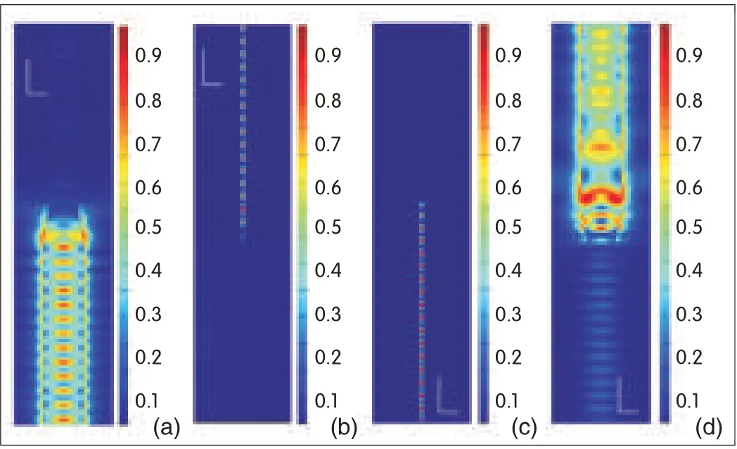
▲Figure 9.Steady state electric field intensity distributions of(a)the input silicon waveguide,(b)the plasmonic-slot waveguide that overlaps above the inputsilicon waveguide,(c)the plasmonic-slot waveguide that overlaps above the output silicon waveguides,and(d)the output silicon waveguide.The horizontals in the 90°angle in(a)-(d)are a scale of 200 nm,and the verticals are a scale of 1μm.
In this paper,we have proposed a silicon-based high-speed plasmonic phase modulator.The modulator is based on a double-layer vertical distributed structure.The bottom layer comprises two silicon waveguides,which are 400 nm wide and 220 nm high,together with tapers that vary from 400 nm to 300 nm in width and are 1μm long.A 16μm long MDM plasmonic-slot waveguide is laid on the top layer,which overlaps the lower silicon waveguides by about 1μm at each side.The slot is filled with a high second-order nonlinear polymer withγ33of 150 pm/Vat 1550 nm wavelength.The Pockels effect of the polymer is applied for EO modulation.Because of the strong confinement of the metalslot and ultrafast response speed of the Pockels effect,the modulation speed can reach hundreds of gigahertz.By introducing a compact,gradually varied taper structure,conversion from photonic modes to plasmonic modes is highly efficient.The feasibility of manufacturing the proposed device has also been discussed.A silicon-based high-speed plasmonic phase modulator is promising for future ultrahigh-speed optical communication networks or silicon interconnects between CMOSchips.
Acknowledgement
This work was supported in part by National Natural Science Foundation of China(61077052/61125504),and Science and Technology Commission of Shanghai Municipality(11530700400).

- ZTE Communications的其它文章
- Introduction to ZTECommunications
- AHistogram-Based Static Error Correction Technique for Flash ADCs:Implementation
- Hardware Architecture of Polyphase Filter Banks Performing Embedded Resampling for Software-Defined Radio Front-Ends
- 1 Tb/s Nyquist-WDM PM-RZ-QPSKSuperchannel Transmission over 1000 km SMF-28 with MAPEqualization
- Compensating for Nonlinear Effects in Coherent-Detection Optical Transmission Systems
- The Key Technology in Optical OFDM-PON