基于串行法的新型EDA優化技術的研究
2015-08-14 21:35:22趙建飛段新文張福祥
現代電子技術 2015年15期
關鍵詞:優化技術
趙建飛+段新文+張福祥
摘 要: EDA代表了當今電子設計技巧的最新發展方向,利用EDA工具,電子設計師可以從概念、算法、協議等開端設計電子系統,大批工作可以通過計算機完成,并可以將電子產品從電路設計、性能分析到設計出IC版圖或PCB版圖的全部過程在計算機上主動處理完成。但EDA技術在優化方式上,卻存在著一定的弱勢,因此提出串行法新型優化方式,把耗用資源巨大、單時鐘周期內完成的并行執行的邏輯塊分割開,提取出相同的邏輯模塊,在時間上復用該模塊,用多個時鐘完成相同的功能,從而在一定程度上解決EDA技術優化不足的問題。
關鍵詞: 電子設計自動化; 優化技術; 串行化; 生產電路
中圖分類號: TN702.2?34 文獻標識碼: A 文章編號: 1004?373X(2015)15?0110?02
Research on new EDA optimized technique based on serial method
ZHAO Jianfei1, DUAN Xinwen1, ZHANG Fuxiang2
(1. Department of Physics, Qinghai Normal University, Xining 810008, China; 2. Unit 93987 of PLA, Xining 810000, China)
Abstract: EDA represents the latest development trend of electronic design techniques in nowadays. By using EDA tools, electronic designers can design electronic system from concept, algorithms and protocols. A large number of work can be done by computer. The entire process of electronic products from circuit design and performance analysis to design IC layout or PCB layout can be done by computer automatically. Since EDA technique has some weakness in optimized mode, the new serial optimization method is proposed. The logic block with large resource consumption completed and executed in single clock period is segmented to extract the same logic modules. The modules are multiplexed in time. Multi?clock are applied to completing the same function, therefor the problem of EDA technique optimized insufficient can be solved to some extent.
Keywords: EDA; optimized technique; serialization; generation circuit
EDA(Electronic Design Automation,電子設計自動化)是20世紀90年代初從計算機輔助設計(CAD)、計算機輔助制造(CAM)、計算機輔助測試(CAT)和計算機輔助工程(CAE)的概念發展而來的。EDA技術就是以計算機為工具,設計者在EDA軟件平臺上用硬件描述語言VHDL完成設計文件,然后由計算機自動地完成邏輯編譯、化簡、分割、綜合、優化、布局、布線和仿真,直至對于特定目標芯片的適配編譯、邏輯映射和編程下載等工作。本文將會引入一種新型的串行優化方式,從而可以使通過EDA工具進行的電子設計在一定程度上占用的芯片面積更小,速度更快。
1 未優化代碼分析[1]
1.1 部分代碼
未優化代碼如下:
entity pmultadd is
port (clk : in std_logic;
a0,a1,a2,a3: in std_logic_vector (7 downto 0) ;
b0,b1,b2,b3: in std_logic_vector (7 downto 0) ;
yout: out std_logic_vector ( 15 downto 0)) ;
end pmultadd ;
architecture a of pmultadd is
begin
process (clk ) begin
if clk′event and clk=′1′ then
yout <= a0*b0+a1*b1+a2*b2+a3*b3 ;
end if ;
end process ;
end a ;
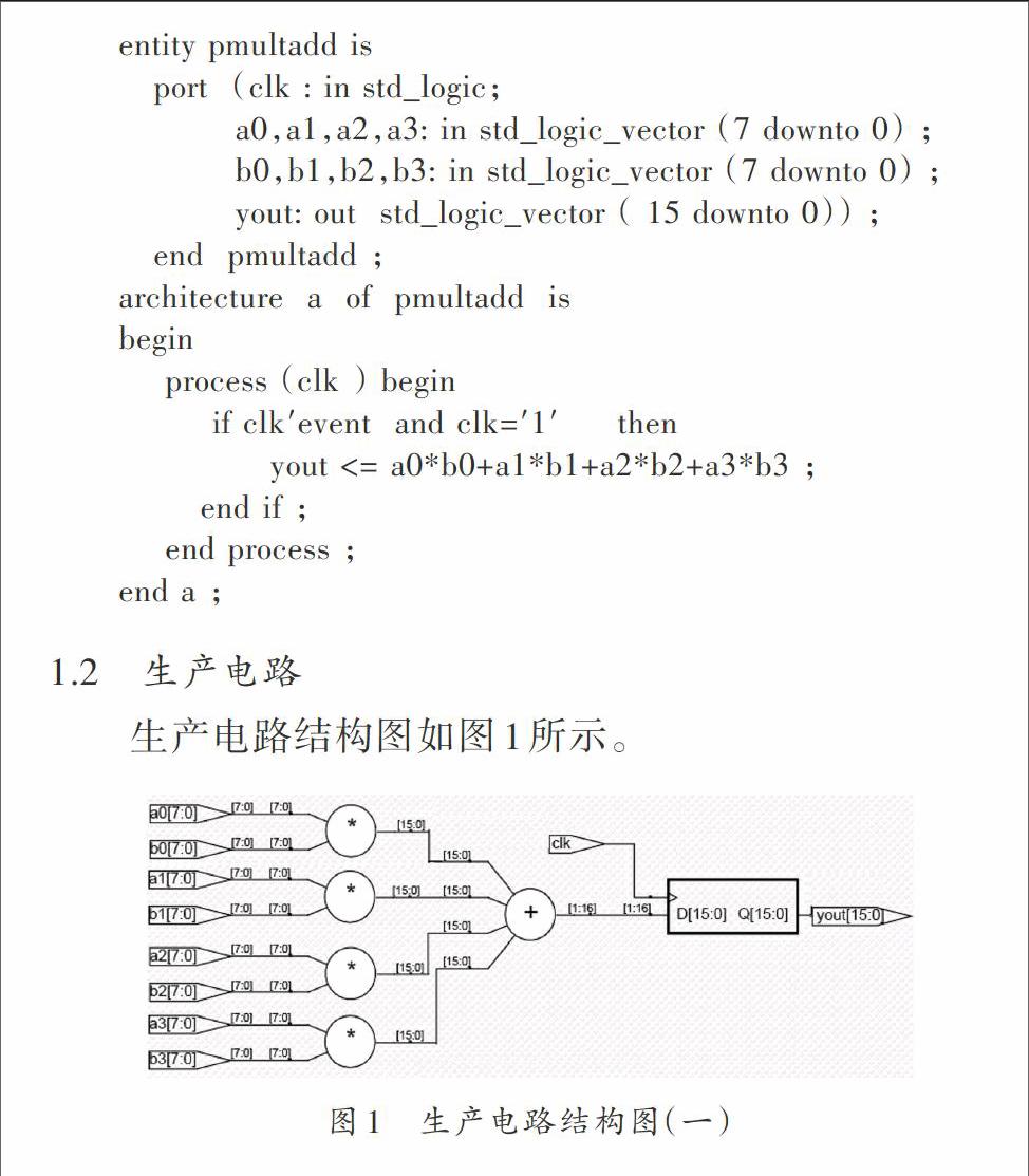
1.2 生產電路
生產電路結構圖如圖1所示。
圖1 生產電路結構圖(一)
綜合結果:適配至EPF10K20TC144?4使用了750個邏輯單元,資源占用率為65%。
1.3 仿真結果
仿真結果示意圖如圖2所示。
圖2 仿真結果示意圖(一)
2 優化代碼分析
2.1 部分代碼
優化代碼分析如下:
entity smultadd is
port (clk,start : in std_logic;
a0,a1,a2,a3: in std_logic_vector (7 downto 0);
b0,b1,b2,b3: in std_logic_vector (7 downto 0);
yout: out std_logic_vector (15 downto 0));
end smultadd ;
architecture a of smultadd is
signal cnt: std_logic_vector (2 downto 0);
signal tmpa,tmpb: std_logic_vector (7 downto 0);
signal tmp,ytmp: std_logic_vector (15 downto 0);
begin
tmpa <= a0 when cnt=0 else
a1 when cnt=1 else
a2 when cnt=2 else
a3 when cnt=3 else
a0;
tmpb <= b0 when cnt=0 else
b1 when cnt=1 else
b2 when cnt=2 else
b3 when cnt=3 else
b0;
tmp <= tmpa*tmpb;
process (clk)
begin
if clk′event and clk=′1′ then
if start=′1′ then cnt<= "000"; ytmp <= (others=>′0′);
elsif cnt<4 then cnt<=cnt+1; ytmp<=ytmp+tmp;
elsif cnt=4 then yout<=ytmp;
end if;
end if;
end process;
end a;
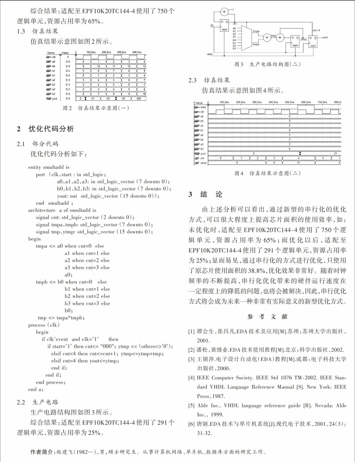
2.2 生產電路
生產電路結構圖如圖3所示。
綜合結果:適配至EPF10K20TC144?4使用了291個邏輯單元,資源占用率為25%。
圖3 生產電路結構圖(二)
2.3 仿真結果
仿真結果示意圖如圖4所示。
圖4 仿真結果示意圖(二)
3 結 論
由上述分析可以看出,通過新型的串行化的優化方式,可以很大程度上提高芯片面積的使用效率,如:未優化時,適配至EPF10K20TC144?4使用了750個邏輯單元,資源占用率為65%;而優化以后,適配至EPF10K20TC144?4使用了291個邏輯單元,資源占用率為25%;顯而易見,通過串行化的方式進行優化,只使用了原芯片使用面積的38.8%,優化效果非常好。隨著時鐘頻率的不斷提高,串行化優化帶來的硬件運行速度在一定程度上的降低的問題,也將會被解決,因此,串行優化方式將會成為未來一種非常有實際意義的新型優化方式。
參考文獻
[1] 譚會生,張昌凡.EDA技術及應用[M].蘇州:蘇州大學出版社,2001.
[2] 潘松,黃繼業.EDA技術使用教程[M].北京:科學出版社,2002.
[3] 王鎖萍.電子設計自動化(EDA)教程[M].成都:電子科技大學出版社,2000.
[4] IEEE Computer Society. IEEE Std 1076 TM?2002. IEEE Standard VHDL Language Reference Manual [S]. New York: IEEE Press,1987.
[5] Alde Inc.. VHDL language reference guide [R]. Nevada: Alde Inc., 1999.
[6] 唐穎.EDA技術與單片機系統[J].現代電子技術,2001,24(3):31?32.
猜你喜歡
電腦知識與技術(2017年5期)2017-04-08 12:50:46
科學與財富(2017年3期)2017-03-15 18:23:56
建筑建材裝飾(2016年10期)2017-01-03 10:12:09
電子技術與軟件工程(2016年22期)2016-12-26 16:04:36
商情(2016年42期)2016-12-23 16:51:17
中國高新技術企業(2016年30期)2016-12-20 04:13:45
科技經濟市場(2016年6期)2016-09-03 22:35:07
中國科技博覽(2016年2期)2016-04-25 16:52:12
企業文化·中旬刊(2015年12期)2016-03-09 03:35:56
科技資訊(2015年7期)2015-07-02 19:34:02
