FPGA控制的反激式開關電源的設計
2016-11-25 00:00:00王磊陳鳳騰高君楠
電腦知識與技術
2016年26期
王磊++陳鳳騰++高君楠
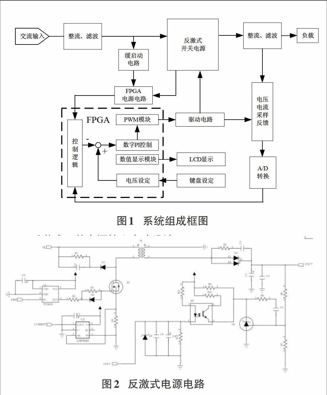

摘要:針對開關電源的特點和現有數字化控制方案,設計了一種以 FPGA為控制核心的反激式開關穩壓電源。文中詳細論述了該系統的硬件組成結構和實現方法,通過改變PWM脈沖寬度實現5-24V輸出電壓可調,具有按鍵設定、電壓顯示、過壓過流保護等功能。以Altera公司的CycloneII系列芯片EP2C5T144C8N為主控芯片,采用Verilog硬件描述語言對PWM信號產生模塊、數字PID模塊、ADC接口邏輯等進行了設計,并在Modelsim仿真軟件上完成了驗證,證明了設計方法的可行性和正確性。
關鍵詞:FPGA;反激式;PWM; PID;Verilog
中圖分類號:TN86 文獻標識碼:A 文章編號:1009-3044(2016)26-0240-03
The Design of Flyback Switching Power Supply Using FPGA Controlled
WANG Lei, CHEN Feng-teng, GAO Jun-nan
(Department of Mechanical and Electrical Engineering,Xuzhou Institute of Technology, Xuzhou 221111, China)
Abstract: According to the characteristics and the existing digital control scheme of switch power supply, a flyback switch power supply with the FPGA as the control core was designed. The hardware structure and the realization method of the system was discussed in detail. Through changing the duty ratio of PWM pulse, it realized voltage range 5~24v;it also has many function such as setting keys, voltage display, over-voltage and over-current protection.The chip EP2C5T144C8N of the Cyclone II series that launched by Altera was the control chip. Verilog HDL language was used in the design of the PWM signal generating module, digital PID module and the ADC interface logic; and then, through simulating on Modelsim software, the correctness and feasibility of the design method was proved.
Key words: FPGA; flyback ; PWM; PID; Verilog
1 引言
變壓器耦合反激式開關穩壓電源,結構簡單,省去了一個和變壓器體積相當的大電感,同時變壓器繞組間相互隔離,“熱地”與“冷地”是絕緣的,其絕緣耐壓強度很大,因而反激式電源在各種強調安全的中小功率電源中得到廣泛的應用[1]。
常規的可調式開關穩壓電源一般采用電位器結合專用的PWM調制芯片TL494、UC3842等,來實現輸出電壓的平緩調節。但是電位器的精度不高,在使用過程中又存在磨損、老化等問題就進一步導致控制精度的下降。數字電位器的出現雖然解決了機械磨損的問題,但受位數及分辨力限制,精度仍不能做到很高[1]。本文采用數控調壓方式,由FPGA邏輯電路產生PWM波控制MOSFET管通斷,進而改變輸出電壓的大小,通過閉環反饋對電壓進行實時精確調整,較好的克服了傳統可調式開關穩壓電源的缺點。此外FPGA器件采用硬件描述語言設計,具有良好的并行處理能力,有效避免了單片機等微控制器運行時程序跑飛的發生,因此系統具有較好的抗干擾能力。……
登錄APP查看全文