某彈上存儲裝置的FLASH陣列無效塊管理可靠性設計
2019-01-10 01:48:14鄭潤
現代電子技術 2019年1期
鄭潤
關鍵詞: 組合塊; 無效塊檢測; 存儲矩陣; 流水線; 可靠性; FLASH
中圖分類號: TN409?34; TP301 ? ? ? ? ? ? ? ? ? ? 文獻標識碼: A ? ? ? ? ? ? ? ? ? ?文章編號: 1004?373X(2019)01?0143?04
Abstract: Since it is difficult to manage the invalid block for FLASH chip storage, the invalid block fast detection and management method under pipeline architecture is proposed to satisfy the performance test requirements of a certain missile storage device, and realize the large?capacity and high?speed storage requirements. The block combination is carried out for the address of FLASH storage matrix, and then the invalid block of the combined storage unit is identified and processed. The lag rewriting method is used to solve the data discontinue storage caused by the unexpected invalid block in engineering application. After the test of related parameters, this method has been successfully applied to a certain missile memory. A large number of experimental results prove that the storage rate and capacity of the storage system can meet the design index, and the system works stably and reliably.
Keywords: combination block; invalid block detection; storage array; pipeline; reliability; FLASH
某彈上存儲器需要對發射前的狀態進行存儲,需存儲的數據量非常大而且存儲過程不能間斷,存儲速率不低于200 MB/s,選用具有體積小、單器件存儲容量大、掉電不丟失、在較惡劣環境下工作可靠等優點的NAND FLASH芯片組成存儲陣列,在雙流水線的架構體系下,進行并行拓展,避免單片NAND FLASH頁編程對存儲時間的限制,擴大存儲容量,提高存儲速度[1]。陣列的無效塊管理問題是高速存儲的難點,若利用傳統單片NAND FLASH的無效塊管理方式進行工程實現,將導致存儲矩陣的驅動程序復雜化,且不能發揮并行讀寫的存儲優勢[2]。
本文提出一種基于組合塊的無效塊管理檢測機制,可以縮短無效塊匹配時間,簡化存儲程序,還能達到多通道之間存儲地址一致,提高存儲速率。
1 ?流水線架構體系硬件設計
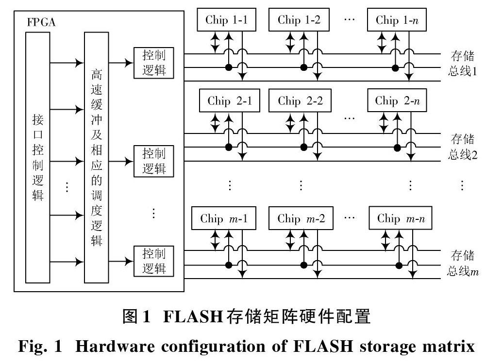
利用NAND FLASH芯片使用特性,將8片芯片的數據端DQ[7:0]以及使能控制端復接到一起,以使能信號和忙閑信號進行區分,構成通道內的流水線結構,如圖1所示。通過主控芯片FPGA的邏輯控制實現5個通道的流水線并行工作,構成5×8的NAND FLASH存儲陣列,最終整個存儲陣列達到200 MB/s的存儲速度,320 GB的存儲容量,完成對單路高數據的高速連續存儲。
2 ?無效塊檢測管理
2.1 ?單片無效塊管理存在的問題
工程中實現大容量高速存儲采用存儲陣列格式、流水線訪問方式進行。對于5×8的NAND FLASH存儲陣列,若采用傳統的逐片進行無效塊檢測,則每個通道都需要一個8 KB的RAM來存儲無效塊列表,5個通道共需要40 KB的RAM,會占據FPGA資源消耗[3];并且無效塊產生的地址隨機,數量不定,使得通道內的流水線操作程序復雜化,同時嚴重影響存儲速度,數據的回讀同樣困難[4],而且影響回讀速率。
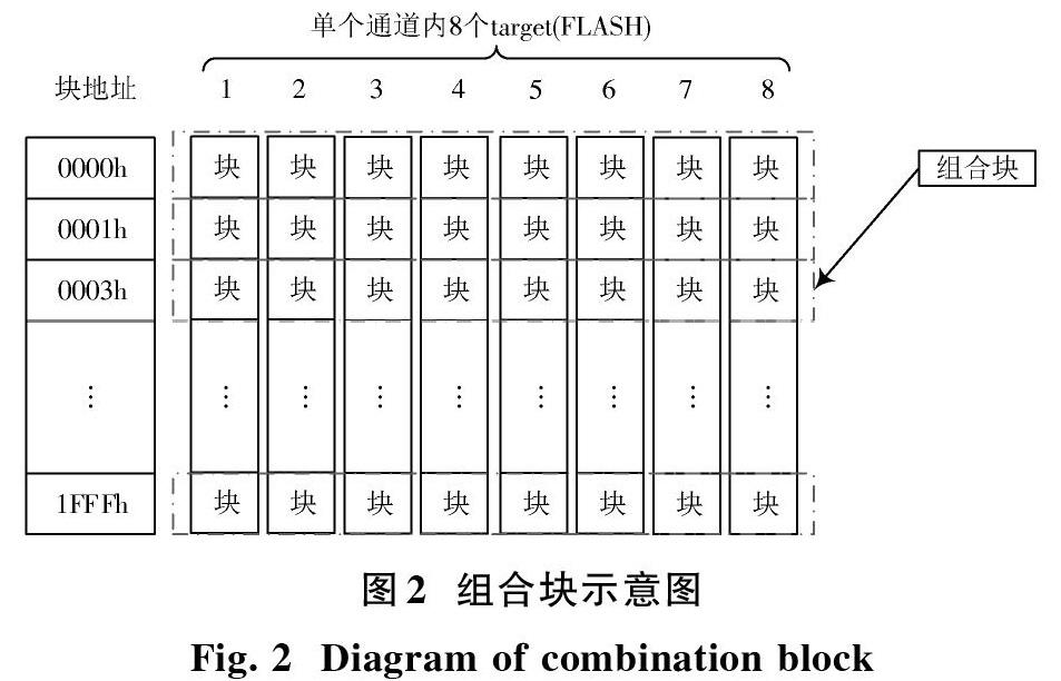
2.2 ?組合無效塊的提出
基于工程實現時的流水線架構,在傳統的單片檢測基礎上,以單個通道作為單元進行劃分,將各個通道內具有相同地址的存儲空間組合起來,建立無效塊查詢列表,如圖2所示,每個虛線框均是一個組合塊。每個通道進行無效塊檢測時以組合塊的地址進行操作,再將檢測結果及時映射至RAM列表中。