In fluence of low-temperature sul fidation on the structure of ZnS thin films?
2019-02-25 07:22:52ShuzhenChen陳書真LigangSong宋力剛PengZhang張鵬XingzhongCao曹興忠RunshengYu于潤升BaoyiWang王寶義LongWei魏龍andRengangZhang張仁剛
Chinese Physics B 2019年2期
Shuzhen Chen(陳書真),Ligang Song(宋力剛),Peng Zhang(張鵬),Xingzhong Cao(曹興忠),Runsheng Yu(于潤升),Baoyi Wang(王寶義),Long Wei(魏龍),and Rengang Zhang(張仁剛)
1 Department of Applied Physics,Wuhan University of Science and Technology,Wuhan 430081,China
2 Institute of High Energy Physics,Chinese Academy of Sciences,Beijing 100049,China
3 University of Chinese Academy of Sciences,Beijing 100049,China
Keywords:ZnS thin films,low-temperature sul fidation,Doppler broadening measurements
1.Introduction
Zinc sul fide(ZnS)is a typical II-VI group compound semiconductor with a direct wide bandgap,for the bulk cubic and hexagonal phases of ZnS,Egis 3.72 eV and 3.77 eV,respectively.[1]ZnS films have a high index of refraction(2.35),high effective dielectric constant(9),and high transmittance in the visible range.[2]ZnS exhibits good biocompatibility and chemical stability in the physiological environment,hence,it can also act as a probe in the medical field.[3,4]ZnS has a high negative conduction band potential,which can effectively reduce water to produce hydrogen;therefore,it can be used as a photocatalytic material.[5,6]ZnS can also decrease window absorption losses and improve the cell short circuit current,and is hence applicable as a buffer layer in solar cells.[2,7]Furthermore,ZnS is widely used in electroluminescent devices such as light-emitting diodes(LED)and flat panel displays.[8-12]
ZnS can be deposited as a thin film by physical or chemical methods.These methods include magnetron sputtering,pulsed laser deposition(PLD),metal-organic chemical vapor deposition(MOCVD),molecular beam epitaxy(MBE),thermal evaporation,electrodeposition,atomic layer deposition(ALD),spray pyrolysis,spin coating,and chemical bath deposition.[13-24]Among these methods,magnetron sputtering has high efficiency and causes no pollution.Films prepared by magnetron sputtering exhibit good interfacial adhesion with the substrate,high compactness,and can be prepared on a large-area substrate.[25,26]
The ZnS film deposited by Du et al.[27]on an indium tin oxide(ITO)substrate by radio-frequency(RF)magnetron sputtering exhibited a characteristic orientation along the(111)crystal plane and no pinhole-like voids.Chalana et al.[28]studied the effects of different substrates on the properties of ZnS-deposited films by RF magnetron sputtering.It was concluded that the metal layer on the substrate had an important in fluence on the deposited ZnS film.Thus,by changing the substrate type,controlled growth of the graded ZnS structure can be achieved using ordinary RF sputtering techniques.Faiazul Haque et al.[25]prepared ZnS thin films by RF magnetron sputtering at different sputtering powers,and found that ZnS thin films grown at 80 W are most suitable for use as buffer layers for photovoltaic applications.Zhang et al.[29,30]successfully prepared ZnS thin films through the vulcanization of ZnO thin films which were prepared by magnetron sputtering in H2S or sulfur vapor atmosphere at 500°C.However,the preparation of ZnS by low-temperature vulcanization and the study of its properties by positron technology has not been reported in the literature.Hence,this study is of significance because it advances knowledge of the vulcanization mecha-nism and explores preparation methods for high-quality ZnS films.
In a previous study where ZnS was prepared by sulfuring Zn,[31]when the temperature was lower than 400°C,Zn did not completely react with S to form ZnS.When the temperature was 500°C,Zn reacted with sulfur to form ZnS.Therefore,the reaction between Zn and S occurs above 400°C.In addition,S has a melting point of 115°C and boiling point of 444.6°C,hence,S melts at 410°C-440°C but is not completely vaporized.Due to this,the remaining sulfur will be more easily solidified during cooling.Therefore,we prepared ZnS films by vulcanizing Zn metal films at a low temperature(below 444.6°C).
2.Experimental details
ZnS thin films were prepared by sulfurizing zinc thin films in sulfur vapor.The zinc thin films were grown on glass substrates from a 99.99%zinc target of diameter 60 mm and thickness 5 mm by RF magnetron sputtering at room temperature.High-purity argon was used as the sputtering gas,and the distance between the target and substrate was 6 cm.The RF power,deposition time,and total pressure were maintained constant at 90 W,2 min,and 1 Pa,respectively.The base of the sputtering chamber was pumped down to a pressure of 1×10⁻⁴Pa before the 15-min pre-sputtering to clean the target surface.After sputter deposition,the as-deposited zinc thin films,together with 20-mg sulfur powder(99.5%of purity),were vacuum-sealed in quartz-glass ampules that had been pumped down to 1×10⁻⁵Pa.These sealed quartz-glass ampules were kept at 200°C for 1 h to enable melting and sufficient diffusion of the sulfur powder throughout the ampules.This was followed by heating 2 h at 410°C,420°C,430°C,and 440°C,the samples for which are labeled A,B,C,and D,respectively.Subsequently,these sealed quartz-glass ampules were cooled in a furnace.After cooling,the remaining sulfur collected at one end of the ampule in the cold zones.The ZnS films were approximately 100-nm thick.
The crystallinity and phase of the thin films were characterized by x-ray diffraction(XRD)using an x-ray diffractometer with CuKα radiation.The surface morphology of the thin films was investigated by scanning electron microscopy(SEM).The microstructure of the thin films was investigated by positron annihilation Doppler broadening measurements with a magnetically guided variable-energy positron beam(0-20 keV).The optical transmission spectra of the films were determined by UV-Vis spectrophotometer in the wavelength range of 200 nm-800 nm.
3.Results and discussion
Figure 1 shows the relative peak intensity of the ZnS(200)and ZnS(111)crystalline planes for samples prepared at various sulfuration temperatures.The respective positions of the diffraction peaks are in agreement with standard data for sphalerite ZnS powders(refer to PDF#05-0566).The diffraction peaks of the ZnS(111)and ZnS(200)crystalline planes are observed at 28.6°and 33.1°,respectively.Figure 1 indicates that the preferred orientation of the ZnS thin films transforms from(200)crystalline planes into(111)crystalline planes with increasing temperature.
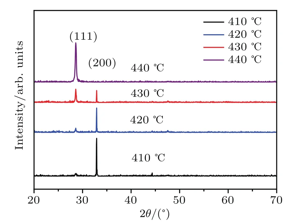
Fig.1.XRD patterns of samples prepared at different sulfuration temperatures.
The grain size of the crystallites was estimated using the Scherrer formula[32]

where D is the average grain size,λ is the incident x-ray wavelength(λ=1.54?A,Kα(Cu)),B is the full width at half maximum(FWHM),and θ is the diffraction angle.
The results are presented in Table 1.
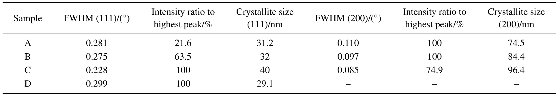
Table 1.Variation in the crystallite size of the samples.
Below the phase transition temperature,the growth structure ofthe ZnS thin film is generally sphalerite,as shown in the XRD spectra.The preferred orientation for sample A is(200)-plane due to its high growth rate.According to the growth theory for an anionic coordination polyhedron,[33]zinc ions in a ZnS crystal which fill the tetrahedral gaps formed by sulfur ions constitute the tetrahedron coordination Zn-S4,including(111)as the anode surface,whose crystal growth rate is the lowest.During the reaction,as the grain size increases,the crystal plane with a high growth rate may disappear.Hence,the low-growth-rate plane becomes prominent.When the sulfuration temperature reaches 440°C,the particles obtain more energy,and the holes shown in Figs.2(b)and 2(c)provide enough space for the particles to move freely.The particles are more likely to aggregate and merge,allowing the film to grow rapidly along the lower direction of free energy.Thus,the(111)crystalline plane replaces the(200)crystalline plane during crystal growth.The grain size of the(111)-plane in Table 1 suddenly drops at 440-°C,indicating that the film grows more densely and the structure tends to be intact.
Figure 2 shows the surface morphology of the ZnS films produced at different temperatures.It is clear that the average grain size of the ZnS films increases with increasing sulfuration temperature.This trend is in agreement with the results presented in Table 1.When the sulfuration temperature is 420°C,the grain size increases and numerous holes begin to appear on the surface,which may be introduced by the melting of zinc.As the melting point of bulk zinc is 419°C,the melting temperature of nanosized metal particles or films is generally lower than the equilibrium point of the corresponding bulk material and decreases significantly as the particle diameter or film thickness decreases.[34]Therefore,the zinc film will melt when the vulcanization temperature is 420°C or higher.According to the vacancy model in the crystal defect model of a liquid metal structure,when a metal crystal melts,a large number of vacancies are formed in the lattice network,so that the liquid metal is easily deformed,and the number of holes increases with increasing temperature.[35]Therefore,at a vulcanization temperature of 420°C,the zinc atoms melt and generate a large number of vacancies,which continuously aggregate with the flow of the liquid metal zinc,eventually forming holes.These holes may lead to a decrease in the highest peak intensity observed by XRD,which is confirmed in Fig.1.Several grains grow along the direction of the holes in sample C when the temperature is 430°C,and the(111)crystalline plane begins to appear.Finally,for sample D,the holes are filled and the small-size grains almost disappear at 440°C.The conversion of Zn to ZnS is kinetically presumed to be a reactive diffusion process involving the surface reaction of Zn with sulfur vapor and boundary reaction of Zn with sulfur diffusing into the ZnS/Zn interface.At a low temperature,zinc may easily melt in the interface of ZnS/Zn.Subsequently,the melted zinc atoms gather at the boundary.Meanwhile,more sulfur tends to be absorbed near the boundary.Therefore up to 430°C,sulfur reacts in the holes originating from the clustering of Zn vacancies.A new ZnS crystal nucleus appears near the prior ZnS grains,which enables grain growth and leads to the preferred orientation ofthe(111)crystalline plane,because the cubic(111)lattice plane has the lowest surface energy.Finally,ZnS continuously fills the holes and the(111)crystalline plane replaces the(200)crystalline plane during crystal growth.
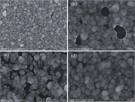
Fig.2.SEM images of the ZnS films produced at(a)410 °C,(b)420 °C,(c)430 °C,and(d)440 °C.In Fig.2(b)and Fig.2(c),there is an accumulation of fluid,which may consist of remnant sulfur around the holes.

Fig.3.EDS profiles of the ZnS films and elemental distribution.
We obtained EDS profiles of the ZnS films prepared by vulcanization at 410°C,420°C,430°C,and 440°C.Our results show that the S/Zn atomic ratio of the ZnS thin films is higher than 1.Among the results,we selected a representative one,which is the EDS map of the ZnS film formed by vulcanization at 440°C(Fig.3).By calculation,we obtained an S/Zn atomic ratio of 7.83,indicating the existence of excess sulfur in the prepared sample.Even in our previous papers,[31,36,37]we have demonstrated the existence of residual sulfur on the grain surfaces of ZnS films prepared in sulfur vapor and H2S gas.
Figures 4(a)and 4(b)plot the valence annihilation parameter S versus the incident positron energy,and the relationship between the core annihilation parameter W and incident positron energy of ZnS films deposited on the glass substrate.The implanted depth of the slow positron was calculated by the following equation[38]
where R is the depth from the sample surface(in unit of nm),ρ is the density of ZnS(4.102 g/cm3),and E is the energy of the incident slow positron(in unit of keV).It can be seen that the S or W parameter indicates the formation of ZnS thin films in the positron energy region of 0.18 keV-4.18 keV.Figure 3 shows that the S parameters of the sample B and sample D are the highest and lowest,respectively,while the W parameters of the B-sample and D-sample are the lowest and highest,respectively.This indicates that the sample B has the highest defect concentration and the sample D has the lowest defect concentration.Taken together with Fig.2,at 410°C and only in the range of 0 nm-0.42268 nm on the surface of the film,zinc reacts with sulfur vapor.Hence,the S parameter increases only in the low positron energy region.For sample B,defects introduced by the reaction of surface zinc atoms with sulfur lead to an increase in S-parameters for incident positron energies of 0.18 keV-2.18 keV,and vacancies introduced by the melting of zinc atoms in the film at 420°C lead to an increase in S-parameters for incident positron energies of 2.18 keV-4.18 keV.At a high temperature of 430°C,the surface will transport S atoms,many defects(such as vacancies and interstitial atoms)are introduced,and as the internal reaction progresses,the surface topography constantly changes,thereby introducing more defects(this can be proved by the residual lique fied sulfur in Fig.2(c)).The internal atoms absorb enough energy to enable relatively free atomic migration,thereby allowing the internal reaction to complete.This leads to the formation of a compact and less defective sample.Consequently,the S parameter is very high on the surface of the sample C and drops sharply as the sample depth increases because of the formation of some large-size grains and the area reduction of holes.This can be confirmed from Fig.2(c).At 440°C,most holes are eliminated and the average grain size approaches 100 nm.This indicates that the zinc vacancies may promote the growth of ZnS thin films.The S parameter of the sample D is the lowest among these samples.This indicates that the reaction is complete,a dense film is grown,the microstructure and crystallinity of the film are greatly improved,and the concentration of defects is the lowest in these samples.These results are consistent with the strongest diffraction peak intensity at 440°C in the XRD spectrum.Meanwhile,the W parameter is high,demonstrating that the zinc vacancies are consumed during crystal growth.
The slope of the S-W plot represents the mechanism of positron annihilation after trapping.The S-W plot has been used to determine the number of defect types in materials.[39]The slope of the S-W plot for these samples shows remarkable changes owing to the generation and filling of holes,and only a single type of defect exists in sample D(in Fig.5).
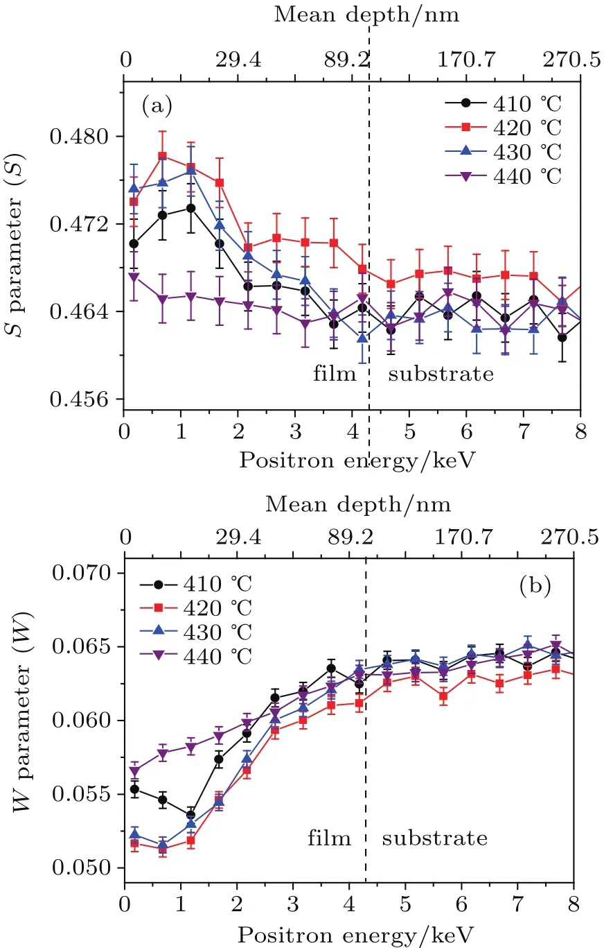
Fig.4.Spectra of the valence electron annihilation parameter S versus the incident positron energy(a),and the core electron annihilation parameter W versus the incident positron energy(b)for ZnS films deposited on glass substrates.
The transmission spectra of the ZnS films are shown in Fig.6.The optical transmission of samples is maintained at 60%-80%in the wavelength range of 400 nm-800 nm.The reduction in optical transmittance can be due to remnant sulfur adhering to the surface of the samples.Zhang et al.also demonstrated that residual sulfur on the surface of the grain causes widening of the absorption edge and a decrease in transmittance.[31]A sharp absorption edge around 340 nm is observed for the films,indicating the conversion of Zn to ZnS above 410°C.When the sulfurization temperature is 430°C,the optical transmission becomes lower than for other temperatures,mainly because of the incomplete growth of the grains.This shows that many defect levels are formed during film growth,and the absorption and scattering effectsare enhanced.After the formation of large grains at 440°C,the film grows more densely,the microstructure and crystallinity of the film greatly improve,the lattice defects reduce,and the absorption and scattering of light weaken,therefore the optical transmission of the ZnS films recovers.
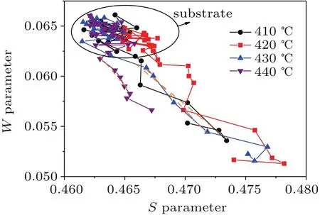
Fig.5.Spectra of the valence electron annihilation parameter S versus the core electron annihilation parameter W for ZnS films deposited on glass substrates.
The transmittance of the film sample obtained by lowtemperature vulcanization in the visible light range is not lower than that of the previously reported ZnS film,which was vulcanized at 500°C;however,the residual sulfur of the former is significantly higher than that of the latter.This phenomenon is very interesting;hence,studying ZnS film materials prepared by low-temperature vulcanization will be our next research focus.
The band energy for all samples from the transmittance spectra can be calculated by formula.[40]The absorption coefficient is given by:
where T and d are the transmittance and thickness,respectively,of the ZnS thin films.Egcan be obtained using Tauc’s relationship:

where A is a constant,hν is the photon energy,and Egis the band gap energy.The band energy is determined from the curve of the variation of(αhν)2with photon energy.The curves for all samples are shown in Fig.7.Thus,we can estimate Egas 3.490 eV,3.479 eV,3.479 eV,and 3.517 eV for ZnS thin films at 410°C,420°C,430°C,and 440°C respectively.Naturally,the band gap energy of the sample B is close to that of sample C.Moreover,in Fig.4(b),the W(E)plots of sample B and sample D are similar.This may signify that holes of different shapes and sizes have the same in fluence on the ZnS structure,which is decisive role of the band energy.The band gap energy of sample D is the highest among these samples.When holes are eliminated,the band energy will approach a normal value.

Fig.6.Optical transmission spectra of samples A,B,C,D.

Fig.7.The variation of(αhν)2 with photon energy of samples A,B,C,and D.
4.Conclusion
ZnS thin films were prepared by sulfuring zinc thin films on glass from 410°C to 440°C.Below the boiling point of sulfur,as the sulfuration temperature increases,the preferred orientation of ZnS thin films changes and holes are generated and filled thanks to the absorption of sulfur near the boundary and melting of Zn metal.The concentration of defects is the lowest when grain growth is nearly complete at 440°C.All of our samples show optical transmissivity over 60%in the visible region.The reduction in optical transmittance and band energy can be attributed to remnant sulfur adhering to the surface of the samples.The band energy of the thin films is the highest at 3.51 eV and decreases to 3.47 eV when there are holes.The findings of this study show that it is possible to produce less-defective ZnS films at a low temperature of 440°C.We will further optimize the structure and properties of ZnS films by changing the vulcanization time at 440°C.
Acknowledgment
The scientific contributions from all of the students in the positron group of the Institute of High Energy Physics are acknowledged here.

- Chinese Physics B的其它文章
- Superlubricity enabled dry transfer of non-encapsulated graphene?
- Synthesis and characterization of β-Ga2O3@GaN nanowires?
- Low-energy(40 keV)proton irradiation of YBa2Cu3O7-x thin films:Micro-Raman characterization and electrical transport properties?
- Preliminary investigation on electrothermal instabilities in early phases of cylindrical foil implosions on primary test stand facility?
- Effects of secondary electron emission on plasma characteristics in dual-frequency atmospheric pressure helium discharge by fluid modeling?
- Nonlinear behavior of the population dynamics of three-level systems in the presence of single photon absorption