Preparation and photoelectric properties of cadmium sulfide quantum dots?
2019-04-13 01:14:42YueGu古月LibinTang唐利斌XiaopengGuo郭小鵬JinzhongXiang項金鐘KarSengTengandShuPingLau劉樹平
Chinese Physics B 2019年4期
Yue Gu(古月),Libin Tang(唐利斌),Xiaopeng Guo(郭小鵬),Jinzhong Xiang(項金鐘),?,Kar Seng Teng,and Shu Ping Lau(劉樹平)
1School of Materials Science and Engineering,Yunnan University,Kunming 650091,China
2Kunming Institute of Physics,Kunming 650223,China
3College of Engineering,Swansea University,Bay Campus,Fabian Way,Swansea SA1 8EN,UK
4Department of Applied Physics,The Hong Kong Polytechnic University,Hong Kong,China
1.Introduction
Semiconductor nanocrystals are usually referred to as quantum dots(QDs),and their diameters vary between 2 nm and 10 nm.This diameter is close to or less than the exciton Bohr radius,resulting in the charge carrier becoming confined in the nanometer regime.Due to the apparent quantum confinement effect,QDs have unique optical and electrical properties.They have great application prospects in optical absorption,photoluminescence and photoelectric conversion,and have been widely used in solar cells,light-emitting diodes(LEDs),photodetectors,photocatalysis and bioimaging.[1–10]The direct band gap of CdS QDs is 2.71 eV and can be used in photovoltaic solar cells,LEDs,displays,etc.Many of these applications require the ability to control the size,shape,surface structure,size distribution,crystallinity,and surface defect of the QDs.At present,there are several methods to prepare QDs,such as organic metal synthesis,template,hydrothermal,co-precipitation,sol–gel and wet chemical methods.[11–16]For example,Bach et al.[17]adopted coprecipitation method to obtain CdS QDs at room temperature after vacuum distillation for 12 h.Kumari et al.[18]synthesized CdSe QDs by continuous stirring for 5 h at high pH level of 11.Cao et al.[3]prepared CdSe QDs by using an improved organometallic synthesis method to dissolve sulfur powder and cadmium oxide in trioctylphosphine(TOP)at 240?C.To date,most of the QD preparation techniques have been carried out under harsh conditions and often require lengthy reaction time and high synthesis temperature.Therefore,these techniques are unsuitable for volume production due to low yield and high cost.In this study,we demonstrated the synthesis of CdS QDs with a wurtzite structure at ambient room temperature and atmospheric pressure by liquid phase synthesis.The as-prepared CdS QDs exhibited uniform diameter and good crystallinity.Compared with existing methods,this method offers many advantages,such as facile preparation,low-cost and controllable QD size.Furthermore,this preparation technique is suitable for volume production and can potentially be applied to synthesize other QDs.This study will make significant contributions to the development of CdS QDs based photodetectors.
2.Experiment
2.1.Chemicals and reagents
Na2S,CdCl2,and NaC12H25SO3were purchased from Tianjin Fengchuan Chemical Reagent Co.Ltd.(Tianjin,China),and the reagents were of analytical grade.
2.2.Fabrication of CdS QDs
Na2S(10 mg/mL)and CdCl2(10 mg/mL)were mixed with an equal volume of colorless transparent sodium alkyl sulfonate(SDS)solution(0.03 mol/mL).Na2S(950μL)was added to 325μL of CdCl2solution at 45?C and allowed them to react for 10 min under room temperature and atmospheric pressure.The supernatant was removed after centrifugation at 3000 rpm for 10 min,ethylene glycol and deionized water(at a ratio of 1:1)were then added.The mixed solution was sonicated for 20 min and centrifuged for a further 10 min.The supernatant was discarded and deionized water was added to the as-prepared yellow CdS QDs.Finally,the CdS QDs were dialyzed(300 MW)for 24 h prior to the fabrication of a photodetector.
2.3.Instrumentation
The morphology and size distribution of the CdS QDs were investigated using transmission electron microscopy(TEM,Tecnai G2F30-TWIN)with an operating voltage of 300 kV.The ultra-violet-visible(UV-Vis)absorption spectra were measured using a U-4100 spectrometer.The x-ray diffraction(XRD)patterns of the samples were acquired using Rigaku D/Max-23.The photoluminescence(PL)and PL excitation(PLE)spectra were measured using photoluminescence spectrometer(Hitachi F-7000).The surface morphology and roughness were studied by atomic force microscope(AFM,Bruker Dimension ICON).The cross-sectional view of the device was investigated by scanning electron microscope(SEM)(NOVA NANOSEM 450).Functional groups on the CdS QDs were studied using Fourier transform infra-red spectroscopy(FTIR,Nicolet iS10).The Raman spectra were obtained using Renishaw in Via Raman microscope with a wavelength of 514.5 nm.The elemental composition of CdS QDs was investigated by x-ray photoelectron spectroscopy(XPS,PHI 5000 Versa Probe II).The images of the interdigital electrodes were observed using Leica optical microscope(DM 2700M).The current–voltage(I–V)curves were measured using a semiconductor device analyzer(Key sight B1500 A).
3.Instrumentation
3.1.Structural and optical characterization
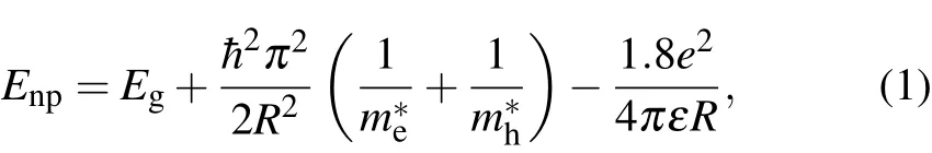
A schematic diagram on the preparation of CdS QDs is illustrated in Fig.1(a).SDS was mixed with Na2S and CdCl2solutions at room temperature and atmospheric pressure,and we allowed them to react for 10 min.SDS was used as surface passivant,which prevented the QDs from aggregating and forming irregular morphologies.The CdS QDs were centrifuged,sonicated and then washed to purification.Figure 1(b)shows the TEM image of the as-prepared CdS QDs revealing spherical shape with excellent dispersibility.HRTEM images of CdS QDs are shown in Figs.1(c),1(d),and 1(e).The measured lattice fringes are 0.196,0.213,and 0.217 nm,which correspond to(103),(110)or(220)of the wurtzite structure,respectively.[19,20]The fast Fourier transform(FFT)patterns in the insets of Figs.1(c)–1(e)also suggest the wurtzite structure of CdS QDs.Figure 1(f)shows the diameter distribution of CdS QDs as shown in Fig.1(a).The size of CdS QDs followed a Gaussian fitted distribution ranging from 2 nm to 7.5 nm with an average diameter of 3.91 nm,the full width at half-maximum(FWHM)was 2.15 nm.SEM images of the CdS QDs are shown in Fig.1(g)and Fig.1(j),which show QDs can be uniformly assembled in the form of thin solid film.However,agglomeration and accumulation of the QDs were also observed.Four random CdS QDs(marked as A,B,C,D)were identified from the AFM image,as shown in Fig.1(h).The height of these four CdS QDs is measured as 1.6 nm,2.6 nm,8.1 nm,and 3.9 nm with an average size of 4.1 nm.It is consistent with the average diameter of 3.91 nm obtained from the size distribution graph in Fig.1(f).
The particle size was estimated from the band gap value using Brus equation by effective mass approximation(EMA)[21–23]
where,Enpis the bandgap of the CdS QDs,Egis the band gap constant,e is the electron charge,m?eis the effective mass of electron(0.19mein CdS),m?his the effective mass of hole(0.8mein CdS),R is the radius of the particle,ε is the dielectric constant(5.7).The calculated Enpvalues are 2.84 eV(R=2.01 nm)and 3.21 eV(R=1.96 nm),which are larger than the bulk value(2.42 eV)due to the quantum effect.
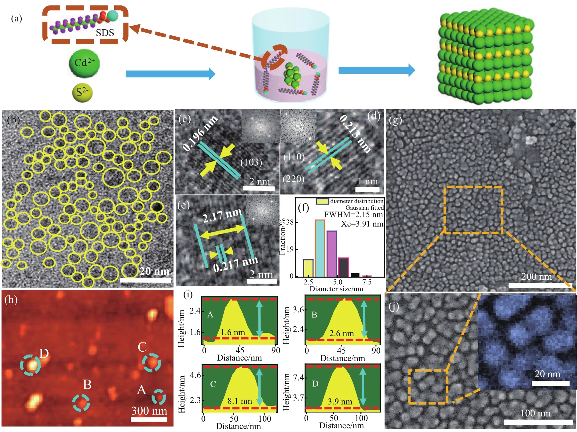
Fig.1.(a)Illustration of the synthesis method to prepare CdS QDs,(b)TEM images of the CdS QDs,(c)–(e)HRTEM images of the CdS QDs,FFT pattern(inset)of single CdS QDs,(f)diameters distribution of the CdS QDs,(g)and(j)the SEM images of CdS QDs,(h)AFM image of the CdS QDs,four QDs are labelled as A,B,C,and D,(i)size measurement of the four QDs in panel(h).
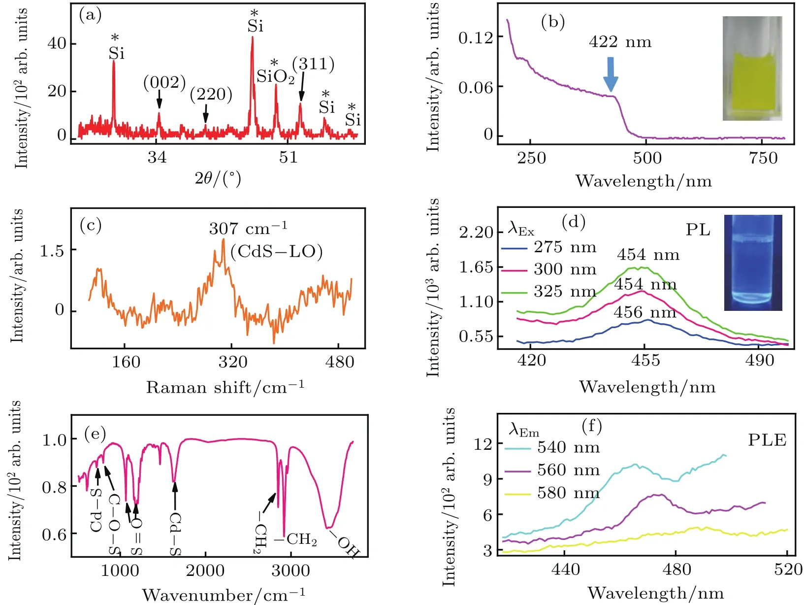
Fig.2.(a)XRD spectrum of the CdS QDs,(b)the UV-Vis absorption spectrum of the CdS QDs,(c)Raman spectrum of the CdS QDs,(d)PL spectra of the CdS QDs solution,(e)FTIR spectrum of the CdS QDs,(f)the PLE spectra of aqueous CdS QDs solution.
The properties of the as-prepared CdS QDs were studied using XRD,Raman,and FTIR techniques,as shown in Figs.2(a),2(c),and 2(e),respectively.Figure 2(a)shows the diffraction peaks at 2θ =34.36?,40.42?,and 52.74?of the CdS QDs,which can be readily assigned to the(002),(220),and(311)planes of the wurtzite structure,respectively.[24]These peaks were comparatively wider than those of the bulk materials due to the finite crystalline size.This is in agreement with the HRTEM results.[25]Si and SiO2peaks,marked by asterisk(*),were also observed in the XRD spectrum due to the presence of SiO2at the surface of the silicon substrate,which the test sample was deposited for characterization.Figure 2(c)shows the Raman spectrum of the CdS QDs,where the basic optical phonon mode(LO)of CdS is situated at 307 cm?1.[26]The FTIR spectrum of the CdS QDs is presented in Fig.2(e). There are two significant stretching of vibration absorption peaks at 723.83 cm?1and 1619.98 cm?1due to Cd–S bonds.The absorption peaks at 1067.93 cm?1and 1196.66 cm?1are related to S–O.The peaks at 802.75 cm?1,2852.32 cm?1,2922.71 cm?1,and 3345.83 cm?1are corresponded to C–O–S,–CH2,–CH2,and–OH,respectively.[27,28]The UV-Vis,PL,and PLE spectra are presented in Figs.2(b),2(d),and2(f),respectively.Figure2(b)shows an absorption peak at 422 nm for the CdS QDs.This demonstrated a blue shift,when compared to the absorption peak of 520 nm for CdS bulk material.This phenomenon is attributed to quantum confinement effect at the CdS QDs.Figure 2(d)shows the PL spectra when the excitation wavelength varies from 275 nm to 325 nm at an interval of 25 nm,the emission peaks are centered at~455 nm.The PLE spectra of the as-prepared CdS QDs are as shown in Fig.2(f).The position of the peaks was obviously red-shifted as the emission wavelength increases,which may be due to the difference in QDs size.

Fig.3.(a)The full-scan XPS spectrum of the CdS QDs,(b)the Cd3d3 and Cd3d5XPS spectra,(c)the S2pXPS spectrum.
To confirm the elemental composition of the CdS QDs,XPS measurement was performed.Figure 3(a)shows a fulls can XPS spectrum of the CdS QDs.It clearly shows the existence of cadmium and sulfur in the as-prepared materials.The main peaks are S2ppeak(167.2 eV),C1speak(284.8 eV),Cd3d3peak(404 eV),Cd3d5peak(411.2 eV),and O1speak(532 eV).The deconvoluted peaks of the two spin–orbit peaks of Cd,namely Cd3d3and Cd3d5,are shown in Fig.3(b),which consisted of 412.46 eV(Cd–S),411.86 eV(Cd–O),405.66 eV(Cd–S),and 405.26 eV(Cd–O).[29,30]The appearance of Cd–O may be due to the surface oxidation of CdS QDs in air.S2ppeak is fitted with three peaks as shown in Fig.3(c),which comprised of 161.66 eV(S–Cd),162.66 eV(S–Cd),and 168.26 eV(S–C).[31,32]The presence of S–C is due to the residual surfactant SDS in the sample.Therefore,the XPS analysis demonstrated the existence of Cd–S bonds in the asprepared QDs and this is consistent with the findings from XRD,Raman,and FTIR studies.
3.2.Optoelectronic properties
According to the UV-Vis spectrum of the CdS QDs,a strong absorption of light is observed at wavelength less than 500 nm and hence an UV detector based on the CdS QDs was fabricated.Figure 4(a)illustrates the fabrication processes of the CdS QDs photodetectors using interdigital gold electrodes as previously reported.[33]The CdS QDs solution was dialyzed(300 MW)for 24 h at room temperature and then drop-cast onto the interdigitated electrodes.This was followed by drying at 70?C for 20 min.Figure 4(d)shows the determination of the optical band gap using UV-Vis spectroscopy.Since CdS is a direct band gap material,the optical band gap can be expressed by Eqs.(2)and(3)

where α is the molar absorption coefficient,h is Planck constant,ν is the incident photon frequency,B is a proportional constant,A is the sample absorbance,b is the sample width,and c is the sample concentration.Based on the calculation,the optical band gap of CdS QDs is Eg=2.71 eV.The result is close to Enp=2.84 eV calculated by Eq.(1).The I–V curve of the UV photodetector irradiated under dark and light conditions( fluorescent lamp,optical power density:114.3 mW/cm2)is shown in Fig.4(e).Under the light condition,the photocurrent increased when compared to that from the dark condition.The responsivity(R)of the photodetector can be expressed by Eq.(4)[34]

where Jphis the photocurrent density and Poptis the optical power density.The responsivity of CdS QDs based photodetector was greater than 0.3μA/W.Presently,this unoptimized value was not large enough but the use of CdS QDs as a UV sensitive material has been demonstrated.

Fig.4.(a)Schematic diagram illustrating the fabrication process of the CdS QDs photodetector,(b)the blank interdigitated electrodes,(c)the interdigitated electrodes containing CdS QDs,(d)optical band gap of CdS QDs,(e)I–V curve,(f)R–V curve.
4.Conclusion
In this study,CdS QDs with narrow size distribution,good crystallinity and excellent dispersibility were prepared using liquid-phase synthesis at room temperature and pressure.The CdS QDs has an optical band gap of 2.71 eV.They were spherical in shape with an average particle size of 3.91 nm.Furthermore,UV-Vis,PL,and PLE studies showed that CdS QDs exhibited strong absorption of light at wavelengths less than 500 nm.Photodetector based on CdS QDs was fabricated to measure the photocurrent under dark and light conditions.The responsivity of this device was found to be greater than 0.3μA/W under light illumination.This simple preparation method is suitable for volume production of QDs,and it has major significance in the research and application of CdS QDs in UV detectors.
[1]Jariwala D,Sangwan V K,Lauhon L J,Marks T J and Hersam M C 2014 ACS Nano 8 1102
[2]Yao G X,Lv L H,Gui M F,Zhang X Y,Zheng X F,Ji X H,Zhang H and Cui Z F 2012 Chin.Phys.B 21 107801
[3]Cao F F,Wang H,Xia Z H,Dai X,Cong S,Dong C,Sun B Q,Lou Y H,Sun Y H,Zhao J and Zou G F 2015 Mater.Chem.&Phys.149 124
[4]Du J H,Xu S H,Wang C L,Pan J Y,Chen J,Zhu L,Lv C G and Cui Y P 2016 RSC Adv.6 77963
[5]Malik H A,Aziz F,Asif M,Raza E,Najeeb M A,Ahmad Z,Swelm W,Zafar Q,Touati F,Kamboh A F H,Supangat A and Sulaiman K 2016 J.Lumin.180 209
[6]Stiffroberts A D 2009 J.Nanophoton.3 031607
[7]Drozdowicztomsia K,Goldys E M,Fu L and Jagadish C 2006 Appl.Phys.Lett.89 113510
[8]Li P,Lan Y,Zhang Q,Zhao Z Y,Pullerits T,Zheng K B and Zhou Y 2016 J.Phys.Chem.C 120
[9]Huang Q T,Hu S R,Zhang H Q,Chen J H,He Y S,Li F M,Weng W,Ni J C,Bao X X and Lin Y 2013 Analyst 138 5417
[10]Feng W,Hang Y,Zhou C H,Mao M,Qian L,Shen H B,Cen Y,Qin Z F,Ma L and Li L S 2016 Biosens.&Bioelectron.77 464
[11]Murray C B,Norris D J and Bawendi M G 1993 J.Am.Chem.Soc.115 8706
[12]Zhu L L,He J,Wang X L,Li D W,He H B,Ren L B,Jiang B W,Wang Yong,Teng C,Xue G and Tao H C 2017 Nanoscale Res.Lett.12 30
[13]Li F,Li W N,Fu S Y and Xiao H M 2015 J.Alloys Compd.647 837
[14]Bach L G,Islam M R,Nga T T,Binh M T,Hong S S,Gal Y S and Lim K T 2013 J.Nanosci.Nanotechnol.13 1970
[15]Majdabadi A,Gaeeni M R,Ghamsari M S and Majles-Ara M H 2015 J.Laser Appl.27 022010
[16]Laatar F,Hassen M,Amri C,Laatar F,Smida A and Ezzaouia H 2016 J.Lumin.178 13
[17]Bach L G,Islam M R,Hong S S and Lim K T 2013 J.Nanosci.&Nanotechnol.13 7707
[18]Kumari A and Singh R R 2017 Physica E 89 77
[19]An L,Wang G H,Zhao L,Zhou Y,Gao F and Cheng Y 2015 Russ.J.Phys.Chem.A 89 1195
[20]Kakati J and Datta P 2013 J.Lumin.138 25
[21]Brus L E 1983 J.Chem.Phys.79 5566
[22]Amma B S,Ramakrishna K and Pattabi M 2007 J.Mater.Sci.Mater.Electron.18 1109
[23]Lu C,Li X,Tang L,Lai S,Rog′ee L,Teng K,Qian F,Zhou L and Lau S 2017 Appl.Phys.Lett.111 063112
[24]Liu L,Xu L L,Zhang H and Chen M 2017 Chin.Phys.B 26 085206
[25]Zhao Q,Xu W and Xu L 2007 Mater.Lett.61 4944
[26]Kumar P,Saxena N,Singh F and Agarwal A 2012 Physica B 407 3347
[27]Rao B S,Kumar,B R,Reddy V R,Rao T S and Chalapathi G V 2011 Chalcogenide Lett.8 177
[28]Rathore K S,Deepika,Patidar D,Saxena N S and Sharma K B 2009 J.Ovonic Res.5 175
[29]Shindov P,Kakanakov R,Philippov P,Anastasova T and Kaneva S 2008 31st International Spring Seminar on Electronics Technology,May 7–11,2008,Budapest,Hungary,p.523
[30]Balcerski W C,Su Y R and Hoffmann M R 2015 Sep.&Purif.Technol.156 915
[31]Rahim M A,Choi W S,Lee H J and Jeon I C 2010 Langmuir ACS J.Surf.&Colloids 26 4680
[32]Hamdi A,Ferreira D P,Ferraria A M,Conceic??ao D S,Vieira Ferreira L F,Carapeto A P,Bou fiS,Bouattour S and Botelho do Rego A M 2016 J.Nanomaterals.2016 11
[33]Tang L B,Ji R B,Li X M,Bai G X,Liu C P,Hao J H,Lin J Y,Jiang H X,Teng K S,Yang Z B and Lau S P 2014 ACS Nano 8 6312
[34]Cai Y H,Tang L B,Xiang J H,Ji R B,Lai S K,Lau S P,Zhao J,Kong J C and Zhang K 2016 Appl.Phys.Lett.109 7433

- Chinese Physics B的其它文章
- Effect of carrier mobility on performance of perovskite solar cells?
- Plasma electrolytic liquefaction of sawdust?
- Insight into band alignment of Zn(O,S)/CZTSe solar cell by simulation?
- Effect of terahertz pulse on gene expression in human eye cells?
- Ultraviolet photodetectors based on wide bandgap oxide semiconductor films?
- A primary model of decoherence in neuronal microtubules based on the interaction Hamiltonian between microtubules and plasmon in the neurons