Thin-film growth behavior of non-planar vanadium oxidephthalocyanine?
2019-08-16 01:20:48TianJiaoLiu劉天嬌HuaYanXia夏華艷BiaoLiu劉標(biāo)TimJonesMeiFang方梅andJunLiangYang陽軍亮
Chinese Physics B 2019年8期
Ti an-Jiao Liu(劉天嬌), Hua-Yan Xia(夏華艷), Biao Liu(劉標(biāo)),Tim S Jones, Mei Fang(方梅), and Jun-Liang Yang(陽軍亮),?
1Hunan Key Laboratory for Super-microstructure and Ultrafast Process,School of Physics and Electronics,Central South University,Changsha 410083,China
2Department of Chemistry,University of Warwick,Coventry,CV4 7AL,United Kingdom
Keywords: organic semiconductor,thin film,vanadyl phthalocyanine(VOPc),growth behavior
1. Introduction
Organic semiconductor film plays an increasingly vital role in next generation thin film devices. Among them, metallophthalocyanines (MPcs) have been widely used as organic functional materials in photoconductive and electroluminescence devices,[1]nonlinear optical devices,[2,3]gas and humidity sensors,[4,5]solar cells,[6,7]organic field-effect transistors,[8,9]organic light emitting diodes,[10]etc. Due to the variety of van der Waals force, MPcs assemble in different stacking structures, inevitably leading to the polymorphs phenomenon.[11]The film morphology and structure greatly influence the device performance.[12,13]Thus,it is very important to grow high-quality MPc film with controllable properties.
Unlike planar MPcs, non-planar vanadyl phthalocyanine(VOPc) presents a pyramidal molecular structure with a C4v symmetry due to the deviation of the center V=O from the molecular plane.[14]Normally, it is more difficult to obtain high-quality VOPc film than planar phthalocyanines. Several techniques have been employed to prepare VOPc film, such as organic molecular beam deposition (OMBD),[15]epitaxial growth,[16]spin-coating,[17]physical vapour deposition,[18]and Langmuir-Blodgett techniques.[19]OMBD is one of the most successful techniques for preparing highly ordered organic film, and the OMBD sublimated VOPc molecules on transparent conductive indium tin oxide (ITO) film, widely used silicon dioxide(SiO2),and flexible kapton substrates are very important for the development of rigid and flexible organic electronics. A deep understanding of VOPc film growth mechanism will provide vital information for fabricating highperformance devices.[20,21]
In this paper, the film growth behavior of non-planar VOPc on the rigid substrates of ITO, SiO2, and the flexible substrate of kapton are systematically studied through atomic force microscope (AFM) and x-ray diffraction (XRD). The VOPc film growth is strongly influenced by the in situ substrate temperature or post-annealing treatment. Meanwhile,3, 4, 9, 10-perylene-tetracarboxylic dianhydride (PTCDA)molecule is used as the templating layer to induce the growth of high-quality VOPc film,and the stacking structure of VOPc coincidentally presents the phase I arrangement.
2. Experimental section
2.1. VOPc film deposition
The polycrystalline VOPc films were prepared by OMBD in a high vacuum chamber(10-5Pa-10-6Pa)on the rigid substrate of ITO,SiO2,and the flexible substrate of kapton. Prior to the film deposition,the substrates were cleaned in an ultra-sonic bath using deionized water, acetone, and isopropyl alcohol for 10 minutes,respectively,and then blown dried with nitrogen. VOPc powder was bought from Aldrich Co. (USA)and used directly.The deposition rate of VOPc film monitored by a quartz oscillator was about 0.1 ?A/s-0.2 ?A/s. The ITO substrate was set at room-temperature, 180°C, and 250°C,respectively. The VOPc films deposited on room-temperature ITO substrate proceed to be annealed for 2 hours at 255°C and 275°C,respectively. The same process except that all of the substrates maintained at room-temperature was employed to grow VOPc film on SiO2or kapton substrate. The PTCDA was deposited via OMBD and used as the template layer for inducing the growth of VOPc.
2.2. VOPc film characterization
The morphologies and height profiles were characterized by AFM (Asylum Research MFP-3D, Santa Barbara, USA)with a tapping mode in air. Wide-angle x-ray diffraction was carried out by an X’Pert PRO (PANalytical, Netherlands) instrument with Cu Kα radiation(α =1.54056 ?A).[22]The rate was set as 0.4°/min to scan from 5°to 28°.
3. Results and discussion
3.1. VOPc film grown on ITO substrate
ITO is well known for its usage as transparent conductive electrode in liquid crystal displays (LCD), organic light emitting diodes(OLED),solar cells,and touch panels.[23]The ITO film coated glass used in this experiment is commercially available, which consists of randomly oriented nanometersize crystal grains resulting from low-temperature(<200°C)of glass substrate in the magnetron sputtering process. In this part, we systematically investigated the growth behavior of vacuum evaporated VOPc films with different film thicknesses,in situ substrate temperature,and post-annealing temperature. Figure 1(a)-1(f) show the AFM morphologies of VOPc film grown on the ITO substrate. The corresponding height profile along the black line is shown below the morphology image.
As shown in Figs. 1(a) and 1(b), the root-mean-square(RMS) roughness becomes larger as the film thickness increases. The RMS roughness of 80-nm-thick VOPc film is 4.99 nm, while for the 160-nm-thick film, the RMS roughness increases to 9.99 nm. In this case, VOPc exhibits an island growth mode since the VOPc molecules are randomly deposited on the disordered VOPc film which has been formed on the ITO substrate, resulting in an increased RMS roughness. It is also found that the 275°C post-annealed VOPc film has larger grains and smaller roughness than the film postannealed at 255°C(RMS is 7.60 nm at 275°C while 9.90 nm at 255°C, as shown in Figs. 1(c) and 1(d)). It is probably because VOPc film is recrystallized during high-temperature annealing to produce larger grain size.
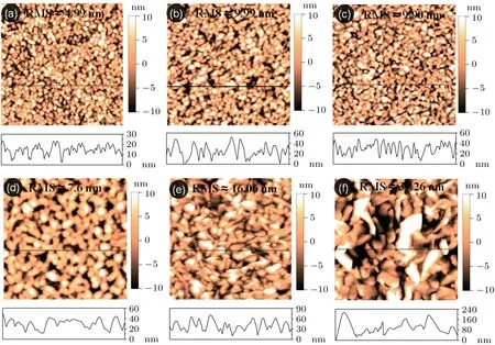
Fig. 1. AFM images showing the morphologies of VOPc thin films grown on the ITO substrate. (a) 80-nm VOPc with an RMS of 4.99 nm, (b)160-nm VOPc with an RMS of 9.99 nm, (c)160-nm VOPc with a post-treatment at 255 °C for 2 hours and with an RMS of 9.90 nm, (d)160-nm VOPc with a post-treatment at 275°C for 2 hours and with an RMS of 7.60 nm,(e)160-nm VOPc deposited at 180°C and with an RMS of 16.06 nm,and(f)160-nm VOPc deposited at 250°C and with an RMS of 37.26 nm.The height profile in each case corresponds to the black lines in the images.
As discussed above, the substrate temperature during vacuum deposition has an important effect on the morphology and structure of the film. Therefore, the ITO substrate is maintained at 180°C and 250°C for comparison during film deposition. Although VOPc grains are arranged irregularly (Figs. 1(e) and 1(f)), the two VOPc films on hightemperature substrate feature larger crystal grains than the films on room-temperature substrate or high-temperature postannealing treatments. Similar to the cases in Figs. 1(c)and 1(d), the crystalline grains of 160-nm-thick VOPc film deposited at 180°C are closely packed, with an RMS of 16.06 nm, while the VOPc film with the same thickness deposited at 250°C exhibits a mixture of platelet-shaped and seed-shaped crystallites. This phenomenon may attribute to longer diffusing distance of VOPc molecules before their nucleation of a stable island, which correspondingly results in a lower island nucleation density and thus larger island sizes. In the present case,the interaction between the organic molecules and the substrate is smaller than that among the organic molecules themselves, thus forming three-dimensional islands (Fig. 1(f)). Pinholes appearing near the small disordered grains can be ascribed to the desorption of VOPc molecules on the high-temperature substrate. The morphologies of the VOPc films prepared by our method differ from that reported in the literature which was lamellae-shaped or step-shaped,[24]probably resulting from the relatively fast deposition rate. It has been reported that VOPc films demonstrate varied grain sizes at the identical substrate temperature by changing the deposition rate.[25]
There are three modes in the crystal growth on a bulk substrate,i.e.,layer-by-layer mechanism(Frank-Vander Mercue), island mechanism (Volmer Weber), and layer-by-layer followed by island mechanism (Stranski-Karstanov).[26]Inspired by the growth theory of inorganic semiconductor,it can be speculated that the VOPc films grown on room-temperature rigid ITO, SiO2, and flexible kapton substrates (VOPc films grown on SiO2and kapton substrates will be discussed below) exhibit the island mechanism. When directly grown on high-temperature (160°C and 250°C) ITO substrate, VOPc film obeys the layer-by-layer followed by island growth. In the process of VOPc vacuum deposition, the gas molecules are physically absorbed on the substrate surface. As time goes on,many three-dimensional cores accumulate on the substrate.Until the condensed crystal nucleus reaches saturation,instead of forming a new nucleus, the newly vaporized molecules of the gas phase will condense onto the existing nucleus to form crystals. The VOPc nucleus grows to form islands. This threedimensional island structure usually has the crystal of VOPc,so ultimately it becomes microcrystalline. On the 160-°C and 250-°C ITO substrates,owing to the similar lattice constant between VOPc and ITO,the binding tendency of VOPc and ITO substrate is higher than that of VOPc molecules themselves.However,the VOPc film does not spread out on the ITO substrate thoroughly and accompanies with the formation of small crystalline grains because of the roughness of ITO surface.Therefore,the film from the nucleation stage takes only a partially two-dimensional expansion mode and conforms to the layer-by-layer followed by island mechanism. In general,the grain size of VOPc grown on ITO heavily relies on the treatment temperature. Below the critical evaporation temperature of VOPc film, higher temperature leads to longer molecules diffuse length on the substrate and larger domain size.
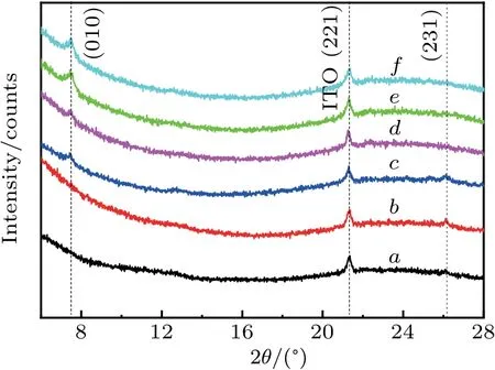
Fig.2. XRD curves of VOPc thin films grown on the ITO substrate. Curve a: 80-nm VOPc pristine thin film,curve b: 160-nm pristine thin film,curve c:160-nm VOPc with a post-treatment at 255°C for 2 hours,curve d:VOPc thin film treated at 275 °C for 2 hours,curve e: VOPc deposited at the substrate with a temperature of 180 °C, and curve f: VOPc deposited at the substrate with a temperature of 250 °C.
For understanding the molecular assembly in VOPc film,XRD measurements are performed. Figure 2 is XRD patterns of VOPc films grown on the ITO substrates under different conditions. Curve a in Fig. 2 shows XRD curve of 80-nm VOPc film deposited on room-temperature ITO. The diffraction peak located at 2θ =21.3°is assigned to the(221)plane of ITO, and it could be used as a diffraction peak for comparison. Another relatively weak diffraction peak located at 26.13°(d=0.34 nm)is indexed as(231)lattice plane of VOPc(phase I type,[27]monoclinic structure, space group P21/c,a=1.42 nm, b=1.31 nm, c=1.27 nm, β =103.2°, and γ = α = 90°). It is suggested that VOPc molecules prefer to grow in the crystalline structure of phase I on roomtemperature ITO.Meanwhile,the really weak diffraction peak indicates that the VOPc film grown on room-temperature ITO is poorly crystalline. As the thickness of VOPc increases to 160 nm,the VOPc film takes a similar crystalline structure for the characteristic diffraction peak is almost preserved (curve b). For the 160-nm-thick VOPc films post-annealed at 255°C on the ITO substrate, it appears a new peak at 7.48°in the XRD diagram,which shows the change of crystalline packing of VOPc (curve c). The 160 nm films show a new diffraction peak at 7.48°with d = 1.18 nm, indexed as (010) of VOPc (phase II type,[28-30]the triclinic structure belongs to space group Pˉ1, a = 1.20 nm, b = 1.25 nm, c = 8.69 nm,α =96.04°,β =94.8°,and γ =68.2°). It means that for the 160-nm-thick VOPc films post-annealed at 255°C, not only the distance of the molecular layer increases,but also another molecular structure (phase II type) emerges. Interestingly, a higher temperature (275°C) treatment can change the crystalline packing of VOPc as well. As shown in Fig.2(curve d),the disappearing diffraction peak of 26.1°indicates that VOPc film shows a single crystalline structure type of phase II at a higher post-annealing temperature, and it has totally changed the VOPc crystalline structure from phase I to phase II compared with the VOPc film deposited on room-temperature ITO.The curves e and f in Fig. 2 show the XRD diffraction patterns of 160-nm-thick VOPc films deposited on 180°C and 250°C ITO substrates, respectively. The only one diffraction peaks at 7.48°clearly indicates that the VOPc molecules are in phase II crystalline structure. It suggests that the VOPc film prepared on in situ 180°C and 250°C ITO substrates are dominated by phase II crystalline structure. In addition,the diffraction peak intensity at 7.48°is significantly enhanced as compared with the films deposited on room-temperature and postannealed, confirming the increased crystallinity in the VOPc films (Fig. 1). Thus, the VOPc films with phase I or phase II can be modulated by the post-annealing and in situ annealing temperature,which will enhance our understanding of the growth behavior of VOPc film on the ITO substrate.
3.2. VOPc film grown on rigid SiO2 and flexible kapton substrate
In order to investigate the effect of substrate material on the growth of VOPc film,we deposit the VOPc molecules on rigid SiO2and flexible kapton substrate by OMBD method.Figure 3 is their AFM morphologies and height profiles.The 80-nm-thick VOPc film grown on the SiO2substrate has an RMS roughness of 5.63 nm, while the RMS of 160-nm-thick film grown under the same condition is 11.06 nm(Figs. 3(a) and 3(b)), which indicates that at the same evaporation rate, the longer deposition time results in a thicker and slightly rougher film. Therefore, it complies with the island growth mode. Influenced by the amorphous state and non-directional property of kapton substrate,the 160-nm-thick VOPc film grown on the kapton features the maximum roughness with an RMS of 12.02 nm. Unlike metals that are provided with a close-packed structure, semiconductors have an open structure.[31]In this open structure, the gap between molecules is relatively greater. Additionally, the voidage of non-planar VOPc molecules after sublimated into film is increased,which is determined by the orientation and saturation of covalent bond. Thus,the increased surface fluctuation leads to a rougher film.
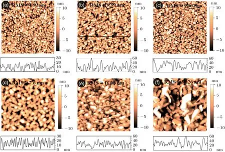
Fig.3. AFM images showing the morphologies of VOPc thin films. (a)80-nm VOPc grown on the SiO2 substrate with an RMS of 5.63 nm,(b)160-nm VOPc grown on the SiO2 substrate with an RMS of 11.06 nm,(c)160-nm VOPc grown on the kapton substrate with an RMS of 12.02 nm,(d)80-nm VOPc grown by PTCDA templating on the SiO2 substrate with an RMS of 5.54 nm, (e) 160-nm VOPc grown by PTCDA templating on the SiO2 substrate with an RMS of 8.31 nm,and(f)160-nm VOPc grown by PTCDA templating on the kapton substrate with an RMS of 10.61 nm. The height profile in each case corresponds to the black lines in the images.
Molecular templating method is widely used to grow high-quality organic semiconductor thin films.[32]Due to the high stability of inducing template layer and good interaction between narrow domains, the size and morphology of target molecules can be strictly controlled. Here, the PTCDA templating layer regarded as a model system in OMBD is used to grow VOPc thin films.[33]As shown in Fig. 3(d), the 80-nmthick VOPc film grown by PTCDA templating on SiO2substrate demonstrates uniformly small grain characteristics with an RMS of 5.54 nm. Then,thicker VOPc film of 160 nm has sublimated on the SiO2substrate by PTCDA templating. Its morphology can be seen from Fig. 3(e). The nano-crystals have grown up during the longer time evaporating process through molecular aggregates or merging neighbouring grains.Therefore, the 160-nm-thick VOPc film grown by PTCDA template has a larger RMS of 8.31 nm than the 80-nm-thick one. However, under the same growth condition, VOPc film grown on PTCDA template layer has a small roughness compared with the VOPc film directly grown on the SiO2substrate. Thus, the PTCDA templating inducing layer is beneficial to improve the film smoothness. The PTCDA templating method is also utilized to prepare VOPc films on flexible kapton substrate. In Fig. 3(f), the 160-nm VOPc film grown by PTCDA templating on the kapton substrate demonstrates enlarged grains than that on the SiO2substrate, and the RMS roughness increases to 10.61 nm. On the surface of unmodified SiO2, due to the interactions between VOPc and polar hydroxyl groups that originate from the oxidation of Si, the molecular diffusion length is shortened and the crystal size decreases. The situation is different for amorphous kapton substrate. Poor interaction between VOPc and kapton contributes to longer molecular diffusion length and facilitates the formation of larger crystals. Similarly, comparing Fig. 3(f)with Fig.3(c),it can be found that the PTCDA template layer is conducive to reduce the roughness of VOPc film.Therefore,on the flexible substrate,relatively uniform and large grain size VOPc film can be obtained, proving that VOPc film can be well applied to flexible devices.
The XRD patterns from VOPc films on the SiO2and kapton substrates are plotted in Fig. 4. Four different peaks at 2θ =6.84°, 7.48°, 13.0°, and 26.13°are indexed as (100),(010),(002),and(231)plane,respectively.The corresponding interstack distances are 12.91 ?A, 11.84 ?A, 6.8 ?A, and 3.4 ?A.For the 80-nm VOPc film grown on the SiO2substrate, a strong diffraction peak located at 7.48°can be observed in Fig. 4(a) (curve 1), corresponding to the (010) lattice plane of phase II with a monlayer of 1.184 nm. Simultaneously,the exclusive appearance of (010) peak indicates that the VOPc molecules preferentially stand on the SiO2substrate,[18,32]and the orientation of the VOPc molecules is presented with the a axis parallel to the substrate surface plane (Fig. 5(a)). The curve 2 in Fig. 4(a) shows the representative XRD curve of 160-nm VOPc film.The main diffraction peaks show a change at 26.13°where this new peak emerges with the film thickness increased from 80 nm to 160 nm. The diffraction peak at 26.13°has d =0.34 nm, indexed as (231) lattice plane of phase I.[34]It means that as the thickness increases, phase II and phase I co-exist,[35]in which phase I is arranged along the geometrical(010)direction,while molecule clusters of phase II are arranged along the geometrical (231) direction. Since the diffraction peak at 7.48°is stronger than 26.13°, most of the VOPc molecular plane is parallel to the(010)direction and partly arranged in the(231)channel with the a axis inclined at 28°to the substrate surface plane,as shown in Fig.5(c). Generally,on the SiO2substrate,the crystalline phases and molecular orientations of the VOPc film are greatly affected by the thin film thickness,which is very different from the VOPc film grown on the ITO.
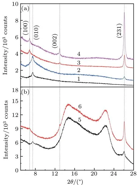
Fig. 4. XRD results of VOPc thin films grown on the (a) SiO2 and (b)kapton substrates, respectively. Curve 1: 80-nm VOPc grown on the SiO2 substrate, curve 2: 160-nm VOPc grown on the SiO2 substrate, curve 3:80-nm VOPc grown by PTCDA templating on the SiO2 substrate,curve 4:160-nm VOPc grown by PTCDA templating on the SiO2 substrate,curve 5:160-nm VOPc grown on the kapton substrate, and curve 6: 160-nm VOPc grown by PTCDA templating on the kapton substrate.
In contrast, the XRD pattern of the 80-nm-thick VOPc films grown on PTCDA template layer is shown by curve 3 in Fig. 4. The most intense peak located at 26.13°suggests that most of the VOPc molecules are arranged in phase I type along the geometrical(231)direction,in which the axis is inclined by 28°with respect to the substrate surface plane.Other VOPc molecules are arranged in the(100)channel with the c axis parallel to the substrate surface plane. The really weak signal of 13.0°diffraction peak indicates just a small part of the molecules lying down on the substrate with the(002)zone parallel to the substrate. As indicated by the molecular orientation in Fig. 5(b), the PTCDA template molecular layer can induce the growth of VOPc thin film with three orientations of phase I. This indicates that a pre-deposited PTCDA template layer can change the crystalline stacking behavior,[36]and tune the molecular orientation from phase II to phase I successfully.Besides,the VOPc films with thickness of 160 nm are formed by the same method. As shown by curve 4 in Fig. 4, the increase of the film thickness does not change the structure of phase I for the VOPc film on the PTCDA template molecular layer,and the peak of 26.1°is significantly enhanced.It means that the molecular orientation arranged along the geometrical channels(231)is enhanced as the thickness increases. Thus,a greater proportion of the VOPc molecules are arranged along the(231)orientations.
Furthermore,the XRD patterns of VOPc films fabricated on the flexible kapton substrate are displayed in Fig.4(b).Owing to the amorphous state of kapton, its baseline is significantly higher than that of the SiO2substrate. On the flexible substrate,the PTCDA template molecular layer can also tune the growth behavior of the VOPc films to phase I structure,which is similar to the SiO2substrate (Figs. 5(c) and 5(d)).This obviously indicates that the structural templating effect exists in both SiO2and flexible kapton substrates, implying that the molecular structure of non-planar VOPc films can be modulated by PTCDA template growth.
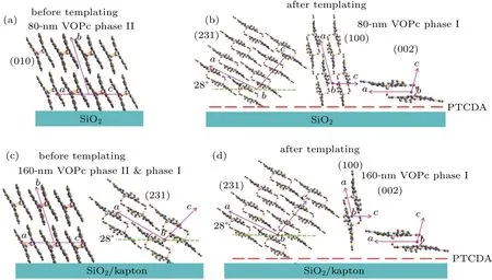
Fig. 5. Schematic of VOPc molecular orientations for: (a) and (b) 80-nm VOPc deposited on SiO2 substrate with and without the PTCDA template layer,(c)and(d)160-nm VOPc grown on SiO2 or kapton substrate with and without the PTCDA template layer.
4. Conclusion
In summary, the growth behaviors of VOPc films on rigid ITO, SiO2substrate, and flexible kapton substrate have been studied with AFM and XRD characterization. The effects on the growth of VOPc film are analyzed and generalized, including the material type of the substrate, in situ and post-annealing temperature, film thickness, and template layer PTCDA. Although the VOPc film deposited on hightemperature substrate or via high-temperature post-annealed treatment has larger grain size,the amorphous and rough ITO surface is not suitable for the formation of VOPc films with high crystallinity.Meanwhile,it is found that the PTCDA template molecule layer contributes to improving the film smoothness and tuning the molecular orientation from phase I to phase II.Furthermore,high-quality and large grain size VOPc films can be formed on flexible kapton substrate,which shows great application potential in flexible electronics. In a word,it is of great significance to realize the controllable and optimal growth of VOPc film because high-quality organic semiconductor film is an indispensable component of improving device performance.

- Chinese Physics B的其它文章
- Exploring alkylthiol additives in PBDB-T:ITIC blended active layers for solar cell applications?
- Study on the nitridation of β-Ga2O3 films?
- Monolithic semi-polar(1ˉ101)InGaN/GaN near white light-emitting diodes on micro-striped Si(100)substrate?
- Spectral properties of Pr:CNGG crystals grown by micro-pulling-down method?
- Quaternary antiferromagnetic Ba2BiFeS5 with isolated FeS4 tetrahedra
- Effects of oxygen vacancy concentration and temperature on memristive behavior of SrRuO3/Nb:SrTiO3 junctions?