Edge-and strain-induced band bending in bilayer-monolayer Pb2Se3 heterostructures*
2021-01-21 02:08:48PengFan范朋GuojianQian錢國健DongfeiWang王東飛EnLi李恩QinWang汪琴HuiChen陳輝XiaoLin林曉andHongJunGao高鴻鈞
Chinese Physics B 2021年1期
Peng Fan(范朋), Guojian Qian(錢國健), Dongfei Wang(王東飛), En Li(李恩),Qin Wang(汪琴), Hui Chen(陳輝),2, Xiao Lin(林曉),2, and Hong-Jun Gao(高鴻鈞),2,?
1Institute of Physics and University of Chinese Academy of Sciences,Chinese Academy of Sciences,Beijing 100190,China
2CAS Center for Excellence in Topological Quantum Computation,Beijing 100190,China
Keywords: Pd2Se3,band bending,lateral heterostructures,scanning tunneling microscope/spectroscopy
1. Introduction
Transition metal selenides have emerged as important two-dimensional (2D) semiconductor candidates for applications of electronics, optoelectronics, and thermoelectric nanodevices.[1–4]The traditional 2D semiconductors that derived from layered bulk materials such as WS2and MoS2have seen a huge advancement in electronics and optoelectronics using all 2D materials.[5–10]Furthermore,layer-dependent band engineering and construction of lateral heterostructures based on 2D materials with different thickness create new possibilities for device applications.[11–14]However, the further development in the field requires the continual investigation of 2D materials systems beyond those that are well known. In addition, creating 2D materials that do not exist as bulk layered materials remains to be fully explored.[15]
Recently, new types of 2D semiconductors without layered bulk counterpart have attracted tremendous attention due to the predicted novel properties beyond the traditional 2D materials.[16–23]Among them, Pd2Se3is regarded to be an ideal optoelectronics material as it exhibits anisotropic transport properties, moderate band gap, and excellent absorption in a wide range of the solar spectrum.[24–26]In experiments,it is impossible to obtain monolayer(ML)and few layer Pd2Se3through mechanical exfoliation due to the lack of layered bulk materials. So far, ML Pd2Se3has been synthesized through phase transformation from bilayer (BL) PdSe2induced by electron irradiation[27–29]or thermal annealing.[30]However,fabricating BL Pd2Se3and studying the thickness dependence electronic properties have not been explored.
Here, we report the construction of BL Pd2Se3islands and BL–ML lateral heterostructures on the graphene-SiC(0001) substrate. By using scanning tunneling microscope/spectroscopy (STM/S), we show a sharp and welldefined zigzag edge formed on the interface between BL and ML Pd2Se3. Band bending and alignment are observed across the interface due to the thickness dependence of the bandgap.In addition, the band bending induced by strain on the deformation can be clearly observed on the confined BL terrace.
2. Methods
The sample was synthesized by molecular beam epitaxy in a commercial ultrahigh vacuum (UHV) STM system with a base pressure of 2.0×10⁻¹⁰mbar. A nitrogen-doped 6HSiC(0001) was flashed to 1550 K, leading to a graphene terminated surface. The atomic beams of Pd(99.95%,Alfa Aesar) and Se (99.999%, Alfa Aesar) were simultaneously deposited at a ratio of ~1:10 by a Knudsen cell(K-cell)evaporator with the substrate maintained at 500 K.Before measurements, the sample was post-annealed at 475 K for 30 min in a Se-sufficient condition. Differential conductance (dI/dV)spectra were acquired by a standard lock-in amplifier at a frequency of 973.1 Hz with a 20 mVrms modulation. The tip calibration was performed on an Au(111)substrate.
3. Results and discussion
The Pd2Se3is thermally transferred from epitaxial BL PdSe2film on graphene through post annealing in vacuum[30](detailed please refer to the method part). The typical largescale STM image in Fig. 1(a) shows that a BL Pd2Se3island is grown on the ML Pd2Se3. The BL Pd2Se3islands are rectangular-shaped with a width of tens of nanometers. A striated Pd2Se3structure with a width of around 1 nm is observed stacked on the top of the BL island.[28]From the line profile along the blue arrow shown in Fig. 1(b), we can get that the height of step edge between the top and bottom Pd2Se3layers is 7.5 ?A (Fig. 1(b)), which is comparable to the value in ML Pd2Se3/graphene(7.3 ?A).
To investigate the interface between two Pd2Se3layers,we got a high-resolution STM image across the step edge and display it in Fig. 2(a). Elliptical dimer protrusions that forming a square lattice (blue box in Fig. 2(a)) are observed on both layers. The lattice constants are a = 5.90 ?A and b=6.03 ?A, which are in agreement with the calculated values of Pd2Se3.[25]There are two groups of Se atoms in the sandwich Pd2Se3structure,which are labeled as SeAand SeB,respectively. The SeBis slightly lower than SeA. The two neighboring SeAatoms are bonding together and form Se-Se dimer structure,while the SBatoms are distributed separately.Therefore,in the STM image,the local density of states of the surface is dominated by SeAatoms forming dimer patterns,while SeBatoms are hardly to be observed due to the lower height than SeAatoms.[30]We superimpose the model of toplayer Se atoms of Pd2Se3onto the STM image, showing that the lattice across the BL and ML Pd2Se3is continuous. Therefore,we conclude that the top Pd2Se3layer is A-A stacked on the bottom layer and the interface between the two layers has a well-defined zigzag type configuration(Figs.2(b)and 2(c)).
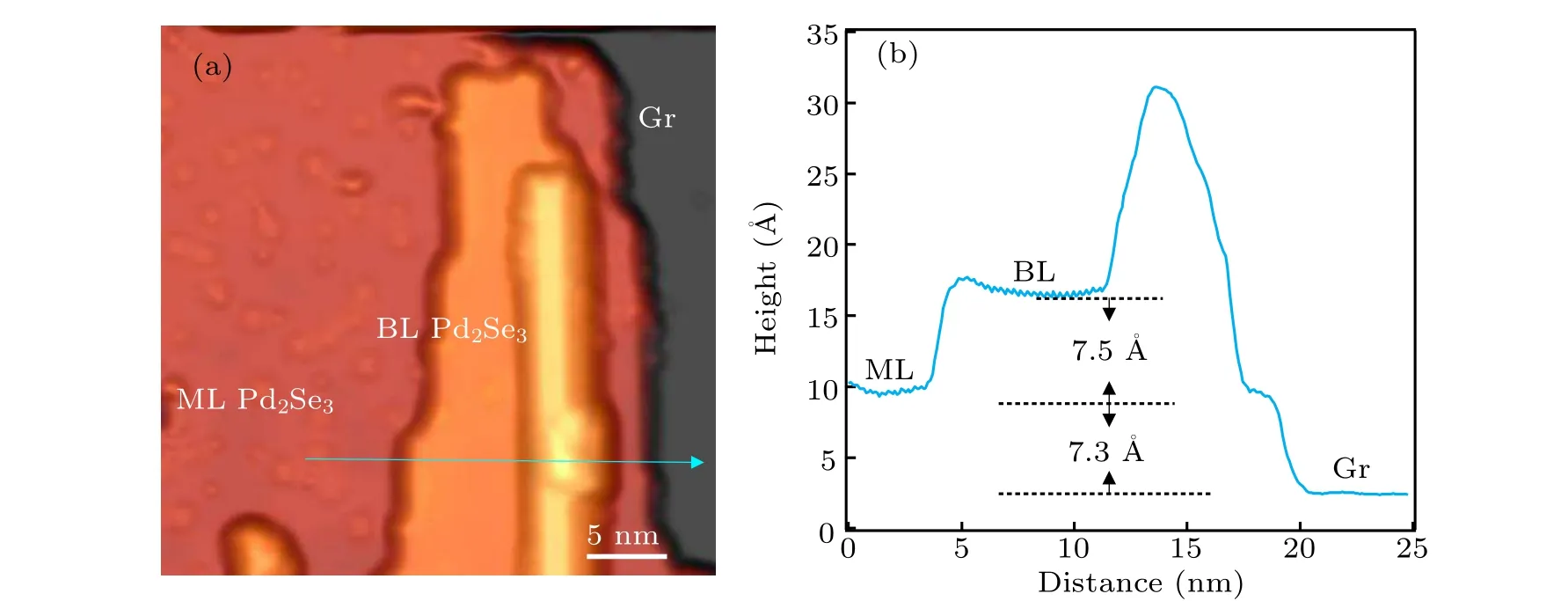
Fig. 1. Construction of BL–ML Pd2Se3 lateral heterostructures. (a) Topographic STM image (VS =-1 V, It =10 pA) showing BL–ML Pd2Se3 lateral heterostructures grown on a graphene/SiC(0001) substrate. (b) Line-profile along the blue arrow in (a), showing the height between two Pd2Se3 layers.
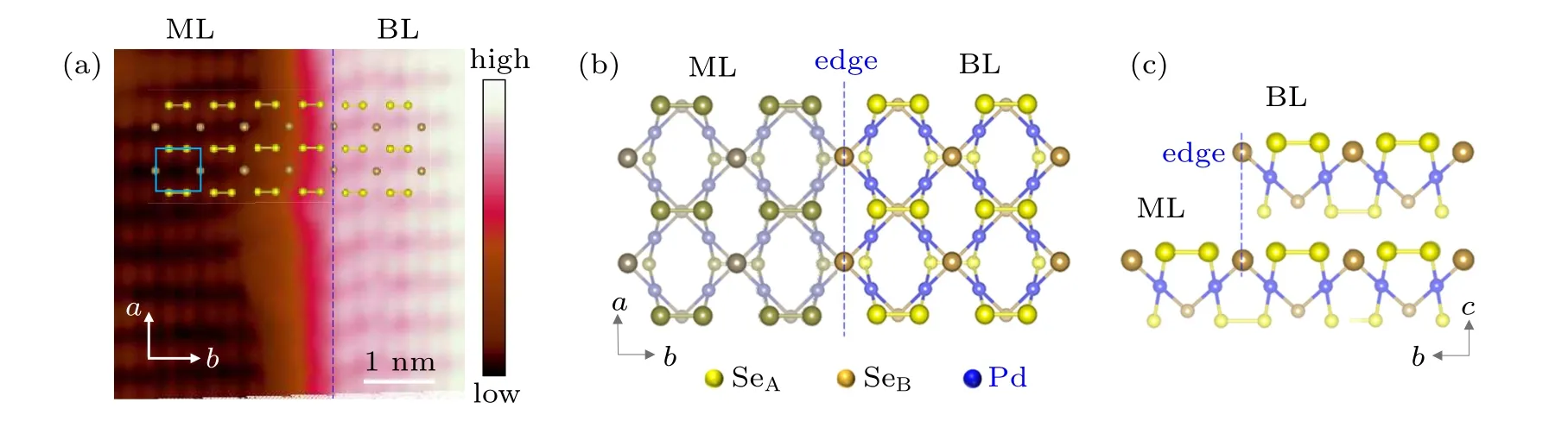
Fig. 2. Atomically sharp interface between BL and ML Pb2Se3. (a) Atomic-resolution STM image (VS =-1 V, It =10 pA) of step edge between BL and ML Pb2Se3. Top view(b)and side view(c)of BL–ML Pb2Se3 lateral heterostructures with zigzag type interface.
To explore the electronic properties of the sharp interface,we collected series of dI/dV spectra across the BL–ML edge as shown in Fig. 3. Figure 3(a) shows the spatial locations where the dI/dV spectra given in Figs.3(b)and 3(c)are carried out. The dI/dV spectra are displayed in a logarithmic scale in Figs.3(b)and 3(c). The numbers on the spectra refer to their positions in the complete set,in which dI/dV spectra are acquired every 0.5 nm from the BL into the ML region,with spectrum #10 acquired at the interface. As the selected dI/dV spectra in Fig.3(c)show,when the tip is far from the interface, the ML Pd2Se3region exhibits a bandgap of about 1.2 eV,while the BL region exhibits a band gap of 1.1 eV.It indicates that Pd2Se3exhibits layer dependent bandgap,similar to the results of PdSe2.[31,32]
The intensity plot of dI/dV spectra in Fig. 3(b) and the selected dI/dV spectra in different regions in Fig.3(c)show the apparent band bending for both conduction band and valence band in the BL region near the interface. The magnitude of the band bending is about 0.17 eV over about 4 nm towards the interface. While the spectra in the ML region,in contrast, exhibit little band bending. It is noticed that pronounced band bending is absent in the edge across ML Pd2Se3and graphene substrate.These results indicate that the ML and BL bulk bands align to form a type-I heterojunction due to the thickness dependence of the bandgap and band edges.[13]
Except for the zigzag edge,the lattice strain induced band bending is also observed in the confined BL Pd2Se3terrace.Figure 4(a)shows a typical confined BL terrace. Several onedimensional structures are observed on its left side,which are attributed to the striated Pd2Se3according to the atomicallyresolved STM images, previous scanning transmission electron microscopy images, and calculations based on density functional theory.[28]On the right side,a grain boundary forms on the ML Pd2Se3,where two different lattice directions highlighted by the red dashed lines and green dashed lines are clearly observed.Therefore,we speculate that the deformation forms on Pd2Se3terrace originates from the spatial confinement between the nanoribbons and grain boundary. In order to clarify the structure of the deformation,we display the zoomin STM image in Fig.4(b),which is the same area highlighted by the black box in Fig. 4(a). We trace the lattice structure by dashed green curves and find that the lattice structure has a slight in-plain bending.
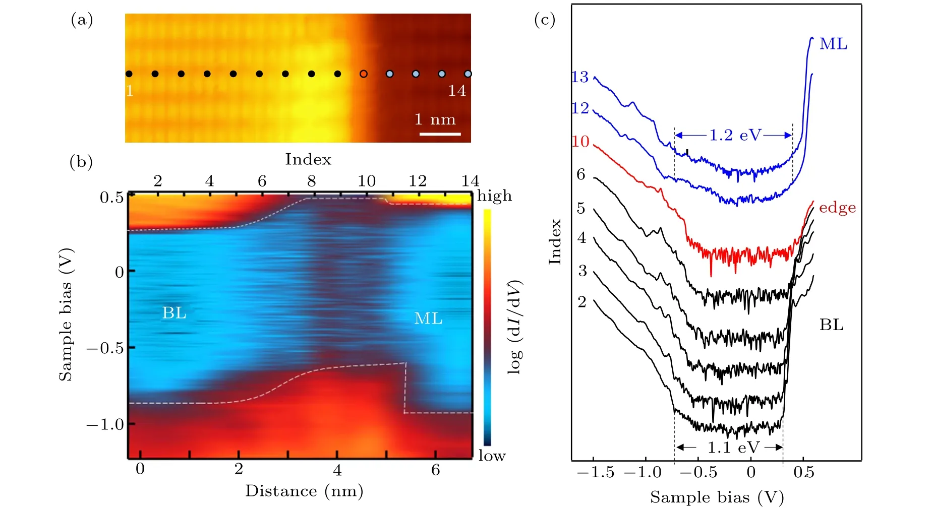
Fig.3. Band profile across the edge of BL–ML Pb2Se3 lateral heterostructures. (a)STM image(VS =-1 V,It =10 pA)of a typical Pb2Se3 edge. The spectra numbers in(b)and(c)are counted from left to right in the path,while spectrum#10 was taken right at the BL–ML interface.(b) Intensity plot of logarithm of dI/dV spectra, imaging the band profile across the interface. (c) Selected logarithm of dI/dV spectra(VS=-1 V,It=100 pA)detected at the colored points in(a),showing the band bending across the interface between BL and ML regions. The edges of valence band,conduct band,and corresponding energy gap in ML and BL regions are highlighted,respectively.
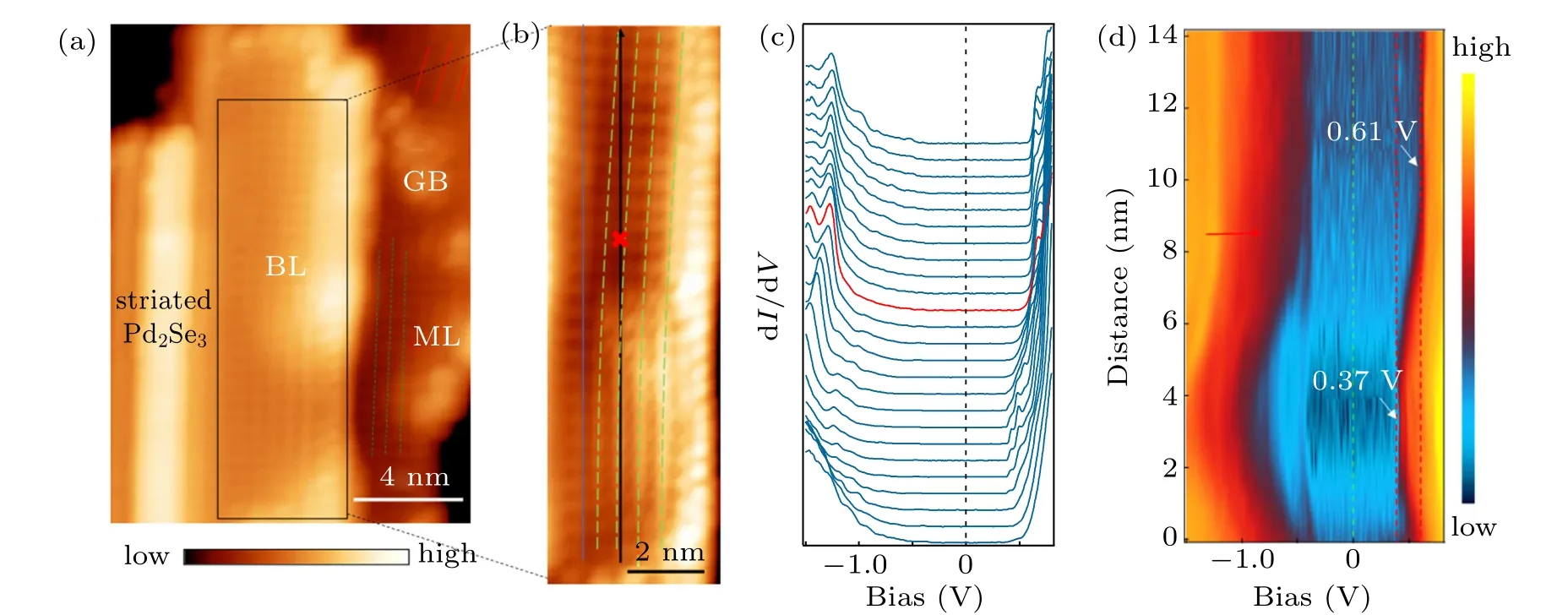
Fig. 4. Strain-induced band bending on a confined BL Pb2Se3 terrace. (a) Topographic STM image (VS = -0.8 V, It = 10 pA) of BL Pb2Se3. The dashed red lines and dashed green lines highlight the lattice directions on the ML Pb2Se3,respectively. (b)Zoom-in STM image(VS =-0.8 V, It =10 pA) of the area marked by the black box in (a). The dashed green lines highlight the in-plane bending of the lattice structure. (c)Waterfall-like plot of 25 dI/dV spectra(VS =-1 V,It =100 pA)detected along the arrowed black line in(b). The red curve is detected at the position marked by red cross in(b),where the strain is released. (d)Intensity plot of(c). The red arrow marks the position where the strain is released. The energy positions of conduction-band minimum at the bending site and strain-free site are labeled.
To investigate the influence of the strain caused by inplane bending,we detect 25 dI/dV spectra and display them as a waterfall-like plot in Fig. 4(c). The bandgap shifts to the valence band when getting close to the deformation and then shifts back towards the conduct band when getting away from deformation. The red curve is detected at the red cross in Fig. 4(b). The bandgap recovers near this site, indicating that the strain is released. Figure 4(d) is the intensity plot of logarithm of Fig.4(c). The intensity pointed by the red arrow corresponds to the red curve in Fig. 4(c). We can clearly see a band bending of the deformation, which indicates that the strain induced by in-plane bending of lattice structure has an n-doping effect. It is worthy to notice that the energy gap of one-dimensional strained Pd2Se3nanoribbons is smaller than 0.05 eV, which should not contribute to such in-plane band bending in the strained Pd2Se3.
4. Conclusion
We have successfully synthesized BL Pd2Se3on graphene-SiC(1000). Our results show the effects of edge and strain on the electronic properties of Pd2Se3. The band of BL Pd2Se3is bending at the ML–BL interface,which forms a heterojunction. For the strain induced by in-plane bending of lattice structure,a n-doped band bending can be clearly observed.Our finding provides several effective ways to develop practical nanodevices based on Pd2Se3heterostructures.

- Chinese Physics B的其它文章
- Numerical simulation on ionic wind in circular channels*
- Interaction properties of solitons for a couple of nonlinear evolution equations
- Enhancement of multiatom non-classical correlations and quantum state transfer in atom–cavity–fiber system*
- Protein–protein docking with interface residue restraints*
- Effect of interaction between loop bases and ions on stability of G-quadruplex DNA*
- Retrieval of multiple scattering contrast from x-ray analyzer-based imaging*