Fractal microstructure of Ag film via plasma discharge as SERS substrates?
2021-12-22 06:42:58XueFenKan闞雪芬ChengYin殷澄ZhuangQiCao曹莊琪WeiSu蘇巍MingLeiShan單鳴雷andXianPingWang王賢平
Chinese Physics B 2021年12期
Xue-Fen Kan(闞雪芬) Cheng Yin(殷澄) Zhuang-Qi Cao(曹莊琪)Wei Su(蘇巍) Ming-Lei Shan(單鳴雷) and Xian-Ping Wang(王賢平)
1Jiangsu Key Laboratory of Power Transmission and Distribution Equipment Technology,Hohai University,Changzhou 213022,China
2Department of Physics and Astronomy,Shanghai JiaoTong University,Shangha 200240,China
3Department of Physics,Key Laboratory of Optoelectronic and Telecommunication of Jiangxi Province,Jiangxi Normal University,Nanchang 330022,China
Keywords: plasma discharge,fractal microstructure,surface-enhanced Raman scattering
1. Introduction
Since the discovery of surface-enhanced Raman scattering (SERS), it has gained significant attention in fields of research and technology for its widespread applications in ultrasensitive sensing.[1–3]It is widely accepted that there are two primary enhancement mechanisms of SERS,i.e., the electromagnetic enhancement(EM)resulting from localized plasmon excitation[4]and the chemical mechanism(CHEM)due to the electron transfer between the target molecules and the metallic particles.[5]Taking advantage of the hotspots, which are usually generated at gaps between nanoparticles (NPs), NPs’junctions and other metallic structures, an enhancement factor up to 108or even larger can be achieved to realize singlemolecule SERS.[6,7]Consequently, various NPs-based SERS substrates composed of orderly or randomly organized NPs,NP dimers, nanorods or nanopillars are proposed to achieve a high density of nano or even sub-nanoscale hotspots.[8–10]However, it should be noted that the size of well-designed hotspots may be too small for some practical applications,whilst larger volume of hotspots is more stable due to the mitigation of the molecular fluctuation effect.[11]Besides,the conventional fabrication strategies suffer some major disadvantages, such as complex operation process, cost inefficiency,time-consuming and low reproducibility. Hence, there is still an urgent demand to develop a simple and economic way of producing stable, robust and large-area SERS substrate. For example, chemical reduction method is applied to the synthesis of indium-silver bimetallic nanocomposites with high enhancement factor,[12]and sandpapers are treated with silver nanoparticles to work as a flexible SERS substrate.[13]Recent efforts have focused on the applications of the atmospheric pressure plasma (APP) in a variety of fields, which is taking place at a breathtaking pace.[14,15]In addition to the high-energy electrons, UV light and shock waves, a high density of reactive radicals such as hydroxyl radicals, atomic oxygen and O3are also generated as plasma interacts with reactant.[16,17]The involved process is rather complicated,while the related mechanism and physics have not been fully clarified. Relevant researches on APP as a potential candidate for the synthesis of nanocomposites and surface modification have been reported recently. For example,Sunet al.[18]proposed the one-step synthesis of AuNP/CNT nanohybrids by using room-temperature direct-current APP. The APP can provide a rapid synthesis method of functional nanocomposites with anti-microbial property.[19]The room temperature plasma is also effective in the substrate washing for dye detection purpose.[20]Besides, Chenet al.[21]adopted the plasma plume formed by the high-speed rotational air fluid in the optimized discharge reactor to remove phenols and p-nitrophenols.
At present, nanoscale silver films of well-controlled thickness and good quality can be manufactured easily. But it is incompetent to be used as an enhanced substrate directly due to the low hotspot density in the one-dimensional structure. A short period of surface modification and etching via APP can be quite effective to change the composition and surface roughness of the target sample simultaneously.For example,Chianget al.[22]used the APP to fabricate the hole-array microstructure for SERS enhancement. However, the trajectory of plasma is controlled by a high-precision numerically controlled stage,which adds the additional complexity. In this paper,fractal microstructures on Ag film via plasma discharge are used for surface-enhanced Raman scattering (SERS). Although fractal theory has been widely applied to many fields,to the best of our knowledge, it is not reported to be observed on plasma treated sample before. Owing to the plasma induced oxidation and ion collision, the surface roughness of the silver film is enhanced with randomly distributed microstructures, which can enhance the Raman sensing. Under positive/negative corona discharge condition, substrates are synthesized and then characterized via scanning electron microscope(SEM),which reveals different patterns due to the switch of electrode and adjustment of the film thickness. Related experiments on SERS measurement show an enhancement factor (EF) of~105via a positive corona discharged thin silver film.
2. Experiments and results
The experiment has three main steps,i.e., the synthesis, the characterization, and the Raman scattering detection.Silver films of 1 cm2are deposited on the silicon wafer by magnetron sputtering (JGP-450A, Sky technology development), which are further treated by the APP to produce the enhanced substrates. Figure 1(a)shows the APP setup,where the plasma ignition is generated by a corona discharge reactor in an open-air environment. One stainless-steel needle electrode of 150 mm in length and 1.80 mm in diameter is placed approximately 1 cm above the sample surface. The air flow of 40 sccm is injected into a tapered quartz tube, which confines the plasma tightly. The voltage amplitude and the polarity of discharge are controlled by a high voltage direct current(HVDC) power source (Teslaman, TCM6000). The needle electrode can act as anode or cathode by tuning the HVDC,resulting in positive/negative corona discharge, respectively.In our experiment, the discharge parameters such as the voltage and the current are fixed at 18 kV and 24 μA, respectively. Typical surface morphologies of 100-nm thick silver films treated under positive/negative corona discharge condition are illustrated in Figs. 1(b) and 1(c). The former condition leads to a more complicated and uneven pattern,which is favorable for SERS applications. Further experiments demonstrate that the film thickness also plays a key role in implementing the surface modification and etching effect. These details are presented and discussed later in Section 3. We are particularly interested in the case of thin film treated by the positive corona discharge,which has not been reported before to the best of our knowledge and is interesting in both fields of SERS and plasma treatment.

Fig.1. (a)Schematic diagram of APP processing. Microscope images of the typical surface morphologies of the SERS substrates under (b) positive and(c)negative corona discharge conditions.
For the SERS measurement, the crystal violet(CV,ACS reagent,≥90.0%)is purchased from Sigma–Aldrich and used as probe molecule. We dilute the CV solution to a concentration of 5×10?5M with Milli-Q water. Then 5 μL of the CV solution is dropped on the center of the substrate surface,followed by a spin coating process at 1000 rpm for 10 s and finally dried at room temperature. A near-infrared Raman spectrometer(Advantage NIRTM,Deltanu)is used to measure the Raman spectra, which is excited by a single mode 785-nm laser. The integration time and resolution of the measurement are 2 s and 2 cm?1,respectively.All the films tested in this paper are approximately 100-nm thick unless otherwise explicitly stated. The repeatability of the experiment is high and all the experimental results are averaged over six measurements.There are many characteristics peaks corresponding to the CV sample, and a specific one around 1172 cm?1is selected for the EF calculation. Details of the spectra of substrates under different treatment times can be found in the following section and the EF calculation can be found in the supplementary material.
The Raman spectra of four different samples are compared in Fig. 2,i.e., thin silver films under positive/negative corona discharge condition, untreated silver film and positive corona discharge treated silicon wafer. There is no obvious characteristic peak around 1172 cm?1in the spectrum that corresponds to the silicon wafer (sample 4), where the only observed characteristic peak around 521 cm?1belongs to silicon. The peak of the target CV is successfully detected from the untreated silver film(sample 3)but the obtained EF is low.The characteristics peaks of CV[23–25]are enhanced via the plasma treated silver films,demonstrating good enhancement ability due to the enhanced surface roughness. The EF corresponds to the positive corona discharged silver film(sample 1)and is approximately 2.3×10⁵,which is one order higher than the substrate treated under negative corona discharge condition(sample 2).

Fig.2. Raman spectra of CV obtained via different SERS substrates. Samples 1 and 2 are positive/negative corona discharge-treated silver films, respectively. Sample 3 is the untreated silver film and sample 4 is positive corona discharged silicon wafer. Treatment time of samples is 9 min.
Figure 3 illustrates the details of the spectra of SERS substrates under different treatment times. It should be noted that the data are obtained by different samples, because it is impossible to remove all of the target CV for a second measurement via the same chip. For each discharge polarity,the treatment time increases from 1.5 min to 9.5 min in steps of 2 min,and the experiments show the enhancement effect of the substrates grows with the treatment time. The linear dependence is suggested in view of Fig.3(c)and the slope that corresponds to the positive corona discharge condition is larger. The data of the treated silicon wafer are not included since no obvious characteristic peak of CV can be observed. Given the same treatment time, the substrate under positive corona discharge condition has a better performance than its counterpart under negative corona discharge condition, taking on different surface patterns as shown in Fig. 1. Our experiment reveals the possibility of generating an effective SERS substrate by using positive corona discharge plasma to modify the surface of simple silver film.
High voltage electrical discharge generates high-energy electrons,UV light,shock waves,and various oxidants. What interact with the APP may involve electron impact, surface oxidation and reactive etching by highly activated species.[26]The enhancement of the substrate treated by APP can be attributed to the changes of the composition and the surface roughness. First, the surface composition of the modified silver films and the reference silicon wafer are characterized with the x-ray photoelectron spectrometer(XPS,EMAX,STREAM-2), which may provide an extra insight into the mechanism behind the interaction between the metallic film and the plasma. It is found that the constituent elements on the film surface are highly position-dependent and we focus on the plasma product,i.e.,the small new structures scatter on the flat film surface after being treated by plasma. For each kind of substrate, six specimens are randomly picked up and then averaged. The statistical results are listed in Table 1,while the details are also provided in the supplementary material.

Fig.3. Time-dependent Raman spectra of silver films treated by(a)positive corona discharge and(b)negative corona discharge. (c)Time-dependent Raman intensity of CV characteristic peak at 1172 cm?1 produced by positive and corona discharges, which are plotted here for comparisons, with dotted line denoting the peak intensity of the untreated silver film.

Table 1. Element composition of plasma products scattered on treated sample surface.
3. Discussion
The silicon element in the substrate can be detected at all the positions and the gold element comes from the spray gold processing before the SEM analysis. We assume that the carbon element originates mainly from the sputtering of carbon from the stainless-steel needle,since the concentration of carbon is greater in samples treated with a negative corona discharge. It should also be mentioned that the weight percentage of elemental silver in the new microstructures that appear after plasma treatment is greater than that of the uncovered silver-film surface. For the positive corona discharged silver film, the nitrogen element has a higher weight percentage in the plasma product,while the carbon element is rich under the negative corona discharge condition. In addition to the difference in the element composition of the plasma products, the SERS performance of the substrates under different plasma polarities relies mainly on their surface patterns. The surface morphologies of the samples performed by scanning electron microscope(SEM,Hitachi,S-3400N)are shown in Fig.4.
As mentioned above, the film thickness and the polarity of discharge are the key conditions and we focus on the surface modification effect of the positive corona discharge plasma on the thin silver film. Comparative experiments are carried out on the negative corona discharged thin film, positive corona discharged thick film and silicon wafer, respectively.By switching the polarity of discharge and adjusting the film thickness, three different kinds of surface morphologies can be observed on the treated silver films. In view of Figs. 4(a)and 4(b), a few compounds due to negative corona discharge distribute randomly on the film surface at first,which turn into the dense random distribution of odd-shaped dots, rods and polygons as time increases. For the case of positive corona discharge,the interaction between the APP and the silver film produces a few lined-up dots at the beginning. Later, these dots are connected into integrity, forming some snake-like irregular curves with considerable length. In the end, these twisted curves form a rather complicated pattern on the surface. The above statement is evident in Figs. 1(b), 4(c), and 4(d). However,the surface morphology under positive corona discharge condition will be different if we increase the film thickness, resulting in the third case. Figure 4(e) shows that many craters are left due to the bombardment of the activated and excited atoms, radicals in the beginning. In Fig.4(f),the accumulation of plasma products on the film surface for longer treatment time can be seen. The thickness-induced difference is consistent with the intrinsic connection between the film thickness and its chemical stability,that is,thinner silver film is more vulnerable to the plasma treatment. For the reference sample,the plasma products on the silicon wafer are rare even for the long treatment time,which can be attributed to the low conductivity of silicon and the surface clean effect of APP.
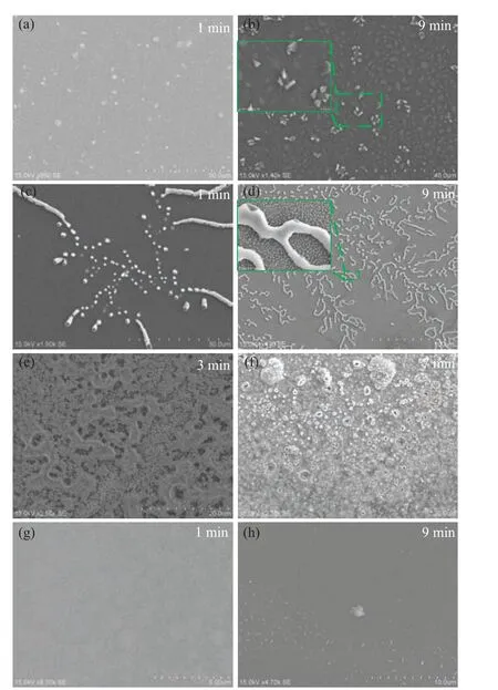
Fig. 4. SEM images of silver and silicon films under different experimental conditions. Treatment time for each sample is illustrated in the upper right corner. [(a),(b)]Thin silver films(100 nm)are treated by negative corona discharge plasma,and[(c)–(h)]samples are treated by positive corona discharge plasma. In panels(c)and(d)silver films are thin(100 nm in thickness). The inset in panel (b) shows the details of odd-shaped particles, and the inset in panel(d)indicates the details of fractal microstructures. In panels(e)and(f)silver films are thick (300 nm in thickness), and panels (g) and (h) show the reference samples of silicon wafer.
Why does the thin silver film(positive corona discharged)work better as an SERS substrate? A concrete analysis is proposed below. The laminar flow in a quartz tube drives the plasma products to the film surface,so does the electrical field under positive corona discharge condition. But the electrical field under negative corona discharge pull these products back to the needle instead. This explains why under the negative corona discharge condition,the interaction products gradually accumulate on the silver film surface with a complete random distribution. Since the particles are separated,the connections among the odd-shaped compounds are few,which reduces the hotspot density. On the contrary,a particle existing on the film surface may significantly change the local electrical field,and thus attracting the new products, falling nearby. Finally,the snake-like microstructures are formed by connecting a group of individual dot-like plasma products gradually. As a result,nanoscale and even sub-nanoscale gaps,i.e., hotspots can be generated in these curved and twisted microstructures.To sum up,the positive corona discharged plasma induces a gradually formed fractal pattern with curved and twisted shapes, which ensures that the aggregation of hotspots enhances the SERS effectively. Since the formation process of the snake-like curves is particularly important for the hotspot aggregation,more details are given in Fig.5. In particular,figure 5(d)clearly shows that some short curves begin to appear due to the connection of small dots. These evidences verify the above-mentioned statements. But the thickness dependence is still unclear. Further discussion is beyond the scope of this paper.
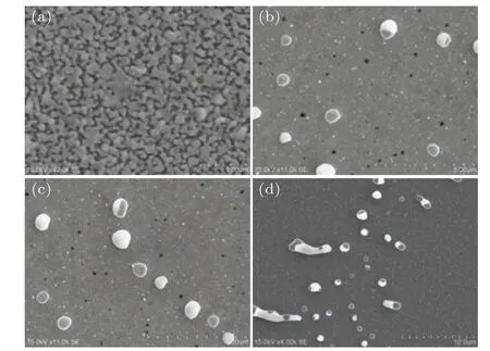
Fig. 5. Formation process of curves via connection of individual dots. The photos are taken on the surface of 100-nm thick silver films treated by positive corona discharge. (a)Surface of untreated silver film;(b)random distribution of dot-like plasma products on film surface;(c)particles begin to line up as a row;(d)short curves appear due to the connection of individual particles.
4. Conclusions
In this work, silver films shortly treated by high voltage electrical discharge are investigated as effective SERS substrates, where the polarity of discharge and the film thickness are recognized as the crucial factors that determine the EF of SERS.Thin film under the short time treatment of positive corona discharge can amplify the Raman scattering signal intensity at least 5 orders and the SEM analysis reveals that the surface patterns under different treatment conditions are completely different. The negative corona discharge leads to random distribution of odd-shaped dots. The positive corona discharge produces the fractal structure formed by snake-like curves, which is gradually built up by connecting individual dots. We suggest that the physics behind this phenomenon may be attributed to the fact that the particles existing on the surface change the local electrical fields of the plasma under the positive corona discharge. Thus connections are more likely to be formed between these particles. The formation process of the fractal structures is important for the large-scale hotspots aggregating on the surface, which ensures the rapid synthesis of SERS substrates with high stability at low cost.

- Chinese Physics B的其它文章
- Modeling the dynamics of firms’technological impact?
- Sensitivity to external optical feedback of circular-side hexagonal resonator microcavity laser?
- Controlling chaos and supressing chimeras in a fractional-order discrete phase-locked loop using impulse control?
- Proton loss of inner radiation belt during geomagnetic storm of 2018 based on CSES satellite observation?
- Embedding any desired number of coexisting attractors in memristive system?
- Thermal and mechanical properties and micro-mechanism of SiO2/epoxy nanodielectrics?