Balanced-switch-current-based modulation strategy for a three-level DC/DC converter with input-parallel-output-parallel structure
2022-02-25 03:24:24LIUDongWUJiahuiCHENZhe
長江大學學報(自科版) 2022年1期
關鍵詞:效率
LIU Dong, WU Jiahui, CHEN Zhe
1.Department of Electronic and Electrical Engineering, University of Sheffield, Sheffield, United Kingdom2.Department of Energy Technology, Aalborg University, Aalborg 9220, Denmark
[Abstract]This paper first discussed the evolution of three-level (TL) DC/DC converters, then introduced the study focus changes from topics of soft switching techniques and the efficiency to the reliability performance of the converter.On this basis, a three-level DC/DC converter (TLDC) consisting of two four-switch half-bridge three-level (HBTL) DC/DC converters with an interleaving and input-parallel output-parallel (IPOP) connection structure was proposed and the topology, operation principle, characteristics, and performances of the proposed converter were analyzed in details.The IPOP structure can effectively reduce the current stresses of main power components, which makes the proposedconverter more applicable for higher power applications.More significantly, by combining the proposed topology with a corresponding periodically swapping modulation (PSM) strategy, not only the currents of two input capacitors can be balanced and greatly reduced, but also the currents of primary-side power switches can be balanced, thus the reliability performance of the converters can be improved.Finally, both simulation and experimental results were presented to verify the proposed converter with a PSM strategy.
[Key words]balanced switch currents; input-parallel output-parallel (IPOP) structure; three-level DC/DC converter (TLDC)
1 Introduction
A three-level (TL)DC/DC converter (TLDC) was first proposed in ref.[1, 2] to reduce the voltage stresses on power switches for higher voltage applications in comparison with the two-level converter. So far, many studies have been conducted on TLDCs[3-6]. In 2004, a novel four-switch half-bridge three-level DC/DC converter (HBTL-DC) was proposed[7], which is more attractive for industrial applications due to its simpler structure and lower cost in comparison with the conventional diode-clamped TLDC[4]. Then, many studies have been conducted based on the four-switch HBTL-DC. Ref.[8] discusses several new solutions to achieve the wide range of soft switching. For high voltage applications, a zero-voltage-switching TLDC with a second-side phase-shift-control is proposed in ref.[9]. Also, to optimize the switching loss and increase the converter’s efficiency, a new zero-voltage and zero-current switching TLDC is proposed in ref.[10]. The above studies mainly focus on the topics of soft switching techniques and the efficiency of the converter.
Recently, more and more studies pay attention to another important design index for the TLDC, i.e., the reliability performance. To ensure the voltages on two input capacitors balancing, a new modulation strategy is proposed for the four-switch HBTL-DC[11]. Ref.[12] proposes a new modulation strategy to balance the currents on input capacitors in four-switch HBTL-DC. In ref.[13], input-parallel output-parallel (IPOP) connected HBTL-DCs with an interleaving control strategy are proposed to improve the reliability of input capacitors by balancing and minimize the currents on them. However, the currents of primary-side power switches in the IPOP TLDCs are unbalanced, which thus causes the unequal distribution of power losses and thermal stresses among them.
This paper proposes a TLDC with an IPOP structure and a corresponding periodically swapping modulation (PSM) strategy. The IPOP structure can effectively reduce the current stresses of main power components, which makes the proposed converter more applicable for higher power applications. More significantly, by combining the proposed topology with a corresponding PSM strategy, not only the currents of two input capacitors can be balanced and greatly reduced, but also the currents of primary-side power switches can be balanced. Finally, the proposed converter with a PSM strategy is validated by both simulation and experimentation results.
2 Topology and operating principle of the proposed converter with a PSM strategy
Fig. 1 shows the topology of the proposed TLDC, which consists of two four-switch HBTL DC/DC converters namely module-1 and module-2. In Fig.1,C1andC2are two sharing input capacitors to split the input voltageVininto two voltagesV1andV2andCois a sharing output filter capacitor. In the module-1,S1,S2,S7,S8andD1,D2,D7,D8are power switches and diodes;Tr1is the isolated transformer;Lr1is the leakage inductance ofTr1;Cb1is the DC-blocking capacitor;Dr1~Dr4are output rectifier diodes;Lo1is the output filter inductor. The structure of module-2 is the same as that of module-1. Besides, in Fig.1,iinis the input current;i1~i8are the currents flowing throughS1/D1~S8/D8;ic1andic2are currents onC1andC2;ip1andip2are currents throughTr1andTr2;iLo1andiLo2are currents throughLo1andLo2;Vcb1andVcb2are voltages onCb1andCb2;ioandVoare output current and voltage;n1andn2are turns ratios ofTr1andTr2.
Fig. 2 presents typically operating waveforms of the proposed converter with a PSM strategy. In Fig. 2,drv1~drv8are driving signals ofS1~S8,d1is a duty ratio in one switching period,Tsis one switching period,Vadis the voltage from pointatod,Vcbis the voltage between pointcandb. Besides, (S1,S2), (S3,S4), (S5,S6), and (S7,S8) are complementary switch pairs. (S1,S3), (S2,S4), (S5,S7), and (S6,S8) are switch pairs having the same driving signal.
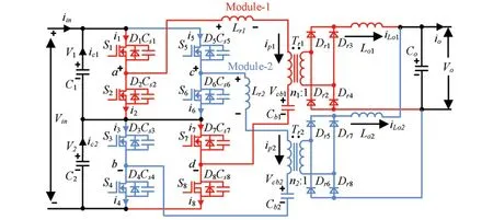
Fig. 1 The structure of the proposed IPOP TL DC/DC converters

Fig. 2 The main operating waveforms with a PSM strategy
To simplify the following analysis, some assumptions are made:
1)Lo1andLo2are large enough to be regarded as the current sources;
2) two modules are identical, i.e.,n1=n2=n;Lr1=Lr2=Lr;ip1= -ip2=ip;
3)iinis regarded as a constant value.
Fig. 3 presents equivalent circuits to illustrate the operating principle of the proposed converter with a corresponding PSM strategy shown in Fig. 2.
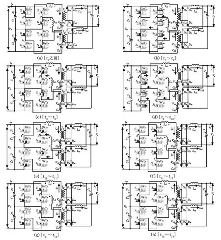
Fig. 3 Equivalent circuits
Stage 0[Beforet7]:S1S3,S6, andS8are all in on-state. For module-I, the power from the input source transfers to the output throughTr1,Dr1, andDr4. For module-II, the power fromCb2transfers to the output throughTr2,Dr6, andDr7. During this stage, the primary currentsip1andip2areio/2nand -io/2n, respectively; and the absolute values ofic1andic2are both |ip1|-|iin|.
Stage 1 [t7~t8]:Att7,S6andS8are switched off. The parasitic capacitorsC6,C8begin to be charged and the parasitic capacitorsC5,C7begin to be discharged. Also,VadandVcbstart to decrease and increase, respectively. During this stage,ip1andip2are kept atio/2nand -io/2n, respectively; and the absolute values ofic1andic2are both |iin|.
Stage 2 [t8~t9]:Att8,C6,C8andC5,C7are charged and discharged toVin/2 and 0, respectively. Also,Vaddecreases toVin/2 andVcbincreases toVin/2. Then, bothD5andD7conduct. Thus,ip1andip2flow throughLr1,Tr1,Lr2,Tr2,S1,S3,D5, andD7. During this stage,ip1andip2remainio/2nand -io/2n, respectively; and the absolute values ofic1andic2are still |iin|.
Stage 3 [t9~t10]:Att9,S1andS3are switched off.C1,C3are charged and the parasitic capacitorsC2,C4are discharged.VadandVcbcontinue to decrease and increase, respectively. Besides,ip1andip2start to decrease and increase linearly, respectively. And they are not enough to provideio, soDr1~Dr8conduct simultaneously. The absolute values ofic1andic2change to |iin|+|ip2|. During this stage, the equations forip1andip2can be expressed as (1) and (2):
(1)
(2)
Stage 4 [t10~t11]:Att10,C1,C3andC2,C4are charged and discharged toVin/2 and 0, respectively. Also,Vaddecreases to 0 andVcbincreases toVin. Then,D2andD4conduct. Thus, in the primary-side,ip1flows throughLr1,Tr1,D2,D7andip2flows throughLr2,Tr2,D4,D5. During this stage,ip1andip2still decrease and increase linearly, respectively; and the absolute values ofic1andic2remain |iin|+|ip2|.
Stage 5 [t11~t12]: Att11,S2S4,S5, andS7are switched on at zero-voltage. Then,ip1andip2flow throughS2,S7andS4,S5, respectively, instead ofD2,D7andD4,D5.
Stage 6 [t12~t13]: Att12,ip1andip2decrease and increase to 0, respectively. Then,ip1andip2change their current directions, i.e., become negative and positive respectively. During this stage, the absolute value ofic1andic2change to |ip2|-|iin|.
Stage 7 [t13~t14]: Att13,ip1andip2decrease and increase to -io/2nandio/2n, respectively. Then,Dr1,Dr4,Dr6, andDr7become off-state. For module-I, the power from the input source transfers to the output throughTr1,Dr2, andDr3. For module-II, the power fromCb2transfers to the output throughTr2,Dr5, andDr8. During this stage,ip1andip2are kept at -io/2nandio/2n, respectively; and the absolute values ofic1andic2are still |ip2|-|iin|.
The analysis of the following half switching period [t14~t21] is similar to that of the half-period [t7~t14], which is not repeated here. It should be mentioned that a corresponding PSM strategy is utilized for the proposed converter, i.e., duty ratios for switches pairsS1,S3,S5,S7and for switches pairsS2,S4,S6,S8are swapped in every switching frequency. Accordingly, the currents on the switchesS1~S8can be balanced in every two switching periods, whose detailed analysis are presented in Section 3.
3 Performances and characteristics
3.1 Voltage stresses on power switches
The voltage stresses onS1~S8are only half of the input voltage (Vin/2) in steady states thanks to the TL structure.
3.2 Duty cycle loss
The duty cycle loss nameddlossin one switching periodTscan be obtained by:
(3)
3.3 Output voltage characteristics
After considering the effect ofdlosson the output voltageVo,Vocan be calculated by:
(4)
where:d1is the duty ratio in one switching period.
3.4 Currents on primary-side power switches
Fig. 4 presents typical waveforms of the currents onS1/D1~S8/D8in the proposed converter with a corresponding PSM strategy.
From Fig. 4, it can be seen thati1~i8are balanced in every two switching periods. Here, only the expression ofi1in two switching periods [t2~t30] is provided as (5):
(5)
According to (5), the root-mean-square (RMS) values ofi1~i8in the proposed converter namelyi1_rms-i8_rmscan be calculated by (6):
(6)
Note: i1~i8 are currents flowing through S1/D1 ~S8/D8, and ic1, ic2 are currents flowing through C1 and C2.Fig. 4 Tyical waveforms of i1~i8 and ic1, ic2
3.5 Currents on input capacitors
In Fig. 4, typical waveforms ofic1andic2are presented. It can be observed from Fig. 4 that the frequencies ofic1andic2are twice the switching frequency thanks to the interleaving control.
According to Fig. 4,ic1andic2in a half switching period can be expressed as:
(7)
Because of utilizing the interleaving control,ip1andip2are just opposite as shown in Fig. 2.ip1andip2in a half switching period can be given as:
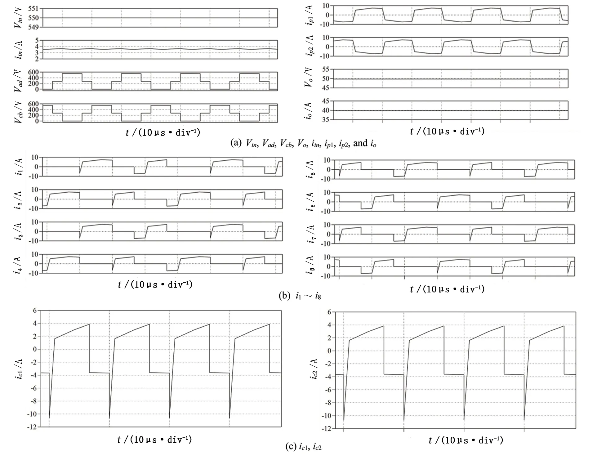
Fig. 5 The simulation results
(8)
Time period [t2~t6] can be calculated as:
(9)
According to (7) ~ (9), RMS values ofic1andic2namelyic1_rmsandic2_rmscan be obtained as:

(10)
4 Simulation and experimental verification
4.1 Simulation verification
A simulation model is built in PLECS to verify the proposed converter with a corresponding PSM strategy. Its circuit parameters are presented in the Appendix.
Fig. 5 presents simulation results includingVin,Vad,Vcb,Vo,iin,ip1,ip2,io,i1,i2,i3,i4,i5,i6,i7,i8,ic1andic2. From Fig. 5, it can be observed thati1~i8are balanced in every two switching periods, and the frequencies ofic1andic2are twice the switching frequency. Besides, the RMS values ofi1~i8are the same (i.e., 4.58A) and RMS values ofic1andic2are also the same (i.e., 3.49A).
4.2 Experimental verification
To verify the proposed converter with a corresponding PSM strategy, a 2kW experimental prototype is also established. Its circuit parameters are listed in Appendix.
Fig. 6 shows the experimental results includingVin,Vo,ip1andip2. From Fig. 6, it can be observed thatip1andip2are just opposite because of the interleaving control.Fig. 7 shows the experimental results includingVad,Vcb,ic1andic2, in which it can be observed thatic1andic2are almost the same and relatively small.

Fig. 6 The experimental results including Fig. 7 The experimental results including Vin, Vo, ip1 and ip2 Vad, Vcb, ic1and ic2
The experimental results ofi1,i2,i7, andi8are shown in Fig. 8, in which it can be observed that their RMS values are almost the same.Fig. 9 shows the efficiencies of the proposed converter, in which the peak efficiency can reach 94.6%.
In summary, the experimental results above are consistent with the theoretical analysis and simulation results, which verify that the proposed converter with a PSM strategy can achieve high efficiencies and effectively balance the currents among the primary-side power switches.
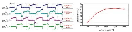
Fig. 8 The experimental results including Fig. 9 The efficiencies results when i1, i2, i7 and i8 Vin = 550V and Vo= 50V 圖8 i1, i2, i7和i8試驗結果 圖9 當Vin=550V和Vo= 50V (逆變器)的效率曲線
5 Conclusion
In this paper, a new TLDC with a corresponding PSM strategy is proposed. The proposed converter is composed of two IPOP connected four-switch HBTL-DCs. Thus, the current stresses of the main power components in the proposed converter can be reduced due to the IPOP structure. Besides, the proposed converter with a corresponding PSM strategy has the following merits: balancing and minimizing the currents on two input capacitors, and balancing the currents among primary-side power switches. Consequently, the improved reliability performances can be achieved. Finally, the effectiveness and validities of the proposed converter with a PSM strategy are verified by both simulation and experimental results.
猜你喜歡
瘋狂英語·初中天地(2021年5期)2021-07-21 02:24:28
甘肅教育(2020年14期)2020-09-11 07:57:42
中學生數理化(高中版.高考數學)(2020年5期)2020-06-02 09:19:08
商周刊(2017年9期)2017-08-22 02:57:49
遼寧經濟(2017年6期)2017-07-12 09:27:16
中國衛生(2016年9期)2016-11-12 13:27:54
時代英語·高二(2015年1期)2015-03-16 00:08:11
中國洗滌用品工業(2015年7期)2015-02-28 19:02:38
電子設計工程(2015年12期)2015-02-27 12:06:10
中國衛生(2014年11期)2014-11-12 13:11:32

- 長江大學學報(自科版)的其它文章
- 壓裂液在火山巖不同類型孔隙中的分布特征
—— 以新疆西泉井區火山巖油藏為例 - 基于高階統計量的砂泥巖薄互層油氣檢測方法
- Three-level LCC resonant DC-DC converter with high-gain modular
- Analysis of the line current differential protection considering inverter-interfaced generation station and countermeasures
- 基于三維連井剖面的地層抗鉆特性參數評價
——以珠江口盆地陸豐區塊為例 - 考慮滑移效應的頁巖基質納米孔隙中壓裂液濾失速度分形計算新模型