Emerging of Ag particles on ZnO nanowire arrays for blue-ray hologram storage
2022-03-12 07:44:38NingLi李寧XinLi李鑫MingYueZhang張明越JingYingMiao苗景迎ShenChengFu付申成andXinTongZhang張昕彤
Chinese Physics B 2022年3期
Ning Li(李寧) Xin Li(李鑫) Ming-Yue Zhang(張明越) Jing-Ying Miao(苗景迎)Shen-Cheng Fu(付申成) and Xin-Tong Zhang(張昕彤)
1Center for Advanced Optoelectronic Functional Material Research,Northeast Normal University,Changchun 130024,China
2Key Laboratory of UV-Emitting Materials and Technology(Northeast Normal University),Ministry of Education,Changchun 130024,China
Keywords: holographic,ZnO nanowires,Ag nanoparticles
1. Introduction
With the rapid development of information communication technology, massive data are exchanged in the Internet every moment. It is estimated that the amount of information generated in the world will reach 175 ZB(zettabyte)in 2025.A big challenge to store large-volume data in photosensitive media efficiently still exists.[1]Compared with electromagnetic storage,optical memory has potential advantages of high density,long life and low power consumption.[2-6]The shorter the wavelength of recording light,the higher the storage density. Holographic technology can use interference fringes to record the whole object information at the Airy disc of photosensitive materials.[7-10]In addition,the“page”mode of holographic recording also provides possibility for a high-speed data transmission.[7]
In recent years, noble-metal/metal-oxide-semiconductor nanostructures have attracted much attention for their excellent photoelectric and chemical properties.[11-20]Especially,the discovery of photochromism in such an inorganic system promotes the development of holographic storage.[21-25]ZnO has advantages of wide band gap, large exciton binding energy and high electron mobility, which make it being a candidate for multifunctional devices.[26]ZnO nanomaterials with wurtzite structure can be made into a variety of morphologies in nanoscale, such as nanorods,[27]nanosheets,[28]and nanotubes.[29]Among them,the regularly arranged ZnO nanowire arrays need no complex preparation process while have large specific surface area afterc-axis oriented growth.[30]So far, nano-Ag/ZnO nanocomposites have been widely investigated in the fields of gas sensors, photocatalysis and photo-electrochemistry.[31-33]Unfortunately,no reports are found on the holographic storage in nano-Ag/ZnO nanocomposite films. As ZnO nanowires (NWs) have low chemical activity on their surface, hot electrons in localized surface plasmon resonance (LSPR) are difficult to transfer from metal to the semiconductor sides.The transition from Ag to Ag+is thus partly inhibited.To resolve the issue,ZnO NWs with oxygen defects are fabricated by hydrothermal method in this paper. Meanwhile, an idea of “electron reverse transfer”is proposed that visible light induces reduction of Ag+ions through the excitation of ZnO. An obvious plasmon spectral enhancement is observed after a blue-ray excitation. Highefficient hologram reconstruction is realized after optimizing nanowire density,oxygen defects and surface roughness.
2. Experimental details
2.1. Preparation of Ag+/ZnO NWs
A two-step hydrothermal method was used to synthesize ZnO NWs. Before preparation, the FTO glass substrates of 2 cm×2 cm were ultrasonically treated in ultra-pure water,acetone and isopropanol for 15 min, respectively, and were dried naturally in air.Meanwhile,in order to remove the residual organic compounds and increase the surface hydrophilicity,the FTO substrate was pretreated with ultraviolet ozone for 15 min. Afterwards,zinc acetate,ethanolamine and methanol were mixed by magnetic stirring at room temperature for 90 min to obtain ZnO seed solution. Then, the ZnO seed solution(50 μL)was spin-coated on the FTO substrate with the speed of 1500 r/min for 30 s. The sample was then placed on a hot plate at 350°C and annealed for 30 min to form a ZnO seed layer. Next, zinc nitrate hexahydrate, polyethylenimine and urotropine(HMTA)were mixed with ultrapure water and stirred at room temperature (300 K) for 60 min to obtain homogeneous ZnO growth solution. Finally,the growth solution and the sample loaded with seed layer were put into a stainless steel reactor and heated in an oven at 95°C for 1 h, 2 h,and 3 h to obtain three kinds of NWs with different lengths.ZnO NWs were then immersed in AgNO3solution of 0.2 M for 10 min in darkness so that Ag+ions can be adsorbed on the NW surface sufficiently. After air-gun drying,Ag+/ZnO NW complexes,named Ag+/ZnO1h,Ag+/ZnO2hand Ag+/ZnO3h,respectively,were obtained. The whole preparation process is shown in Fig.1.
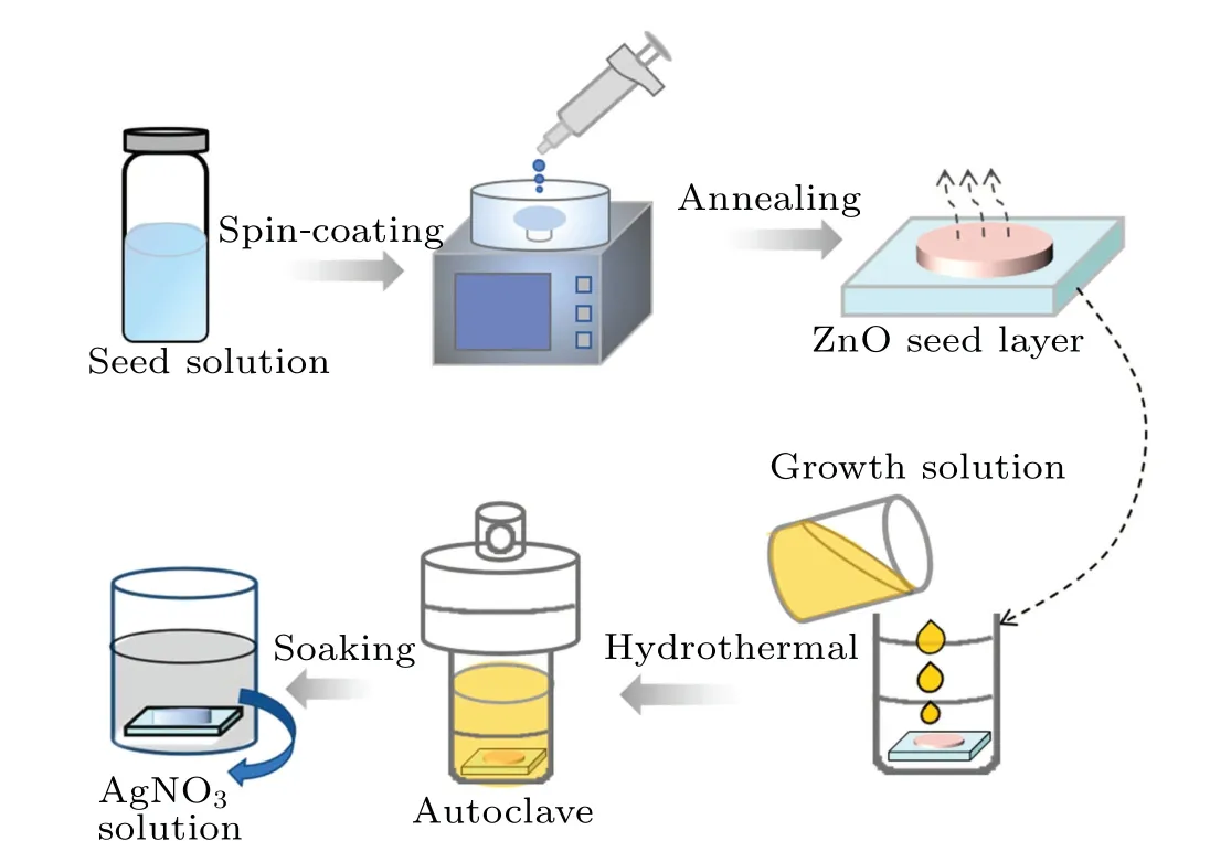
Fig. 1. Preparation process of Ag+/ZnO nanowires composite films.Hydrothermal times are 1 h,2 h and 3 h,respectively.
2.2. Optics setup
The optical devices for holographic kinetics are shown in Fig. 2. Two coherent beams (403.4 nm, 140 mW·cm-2, spolarized) are generated from a blue-violet laser. One of the beams loaded with information is incident on the Ag+/ZnO NW arrays, and the other beam irradiates at the same point of the sample to inscribe holograms. A red laser (671 nm,14 mW·cm-2,s-polarized)is used as a detect source to monitor the formation of holographic fringes. The first-order diffraction signal is recorded on a photodiode which is connected to a computer. The diffraction efficiency of the holographic grating with Fresnel loss can be defined as the ratio of the intensity of the first-order diffraction beam to that of the probe beam passing through the sample.
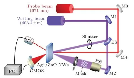
Fig.2. Optical device of Ag+/ZnO nanowire for dynamic recordings in holographic gratings and holograms(M:mirror;BS:beam splitter;PD:photodiode;BE:beam expander).
3. Results and discussion
A scanning electron microscope (SEM) was used to observe the surface morphology of ZnO NWs. The top views of ZnO NWs are shown in Figs.3(a)-3(c),and the cross-sectional views are inserted, correspondingly. ZnO NWs with a good vertical growth state on the FTO substrate is observed. The length of the NWs increases with prolonging hydrothermal time, which is measured to be 300 nm, 600 nm and 750 nm for the hydrothermal times of 1 h, 2 h and 3 h, respectively.From the top view of SEM images,the surface nanowire density is also dependent on hydrothermal time, which is statistically analyzed. The results show that the surface density of ZnO NWs for hydrothermal time of 1 h is the highest,reaching 2.5×1010cm-2. With the increase of hydrothermal time,the surface linear density decreases to 1.74×1010cm-2and 8.3×109cm-2for 2 h and 3 h, respectively. The difference may result from the fact that the ZnO NWs hardly keep growing vertically and uniformly all the time during the hydrothermal treatment process. Thus,some of the NWs cannot be observed on the sample surface. Figures 3(d)-3(f)show the NW diameter distribution and the cumulative percentage of volume fraction. The results show that the average values of NW diameters are 27.62 nm and 31.36 nm for ZnO1hand ZnO2h,respectively. The NW diameter less than 40 nm occupies 97.4%(ZnO1h)and 88.8%(ZnO2h).However,for ZnO3h,the NW diameter increases significantly,almost to 37.81 nm. Therefore,hydrothermal time plays a key role in the longitudinal length and surface diameters of NWs.
X-ray diffraction(XRD)tests were carried out on ZnO1h,as shown in Fig. 4(a). Compared with the standard card of ZnO (PDF #79-0207), it is observed that the prepared ZnO NWs have excellent crystallinity. The diffraction angles of 34.381°and 36.181°correspond to the (002) and (101) crystal planes of wurtzite ZnO,respectively. Disappearance of the(100)diffraction pike that corresponds to the diffraction angle of 31.698°is most possibly resulted from thec-axis orientation growth of ZnO NWs. However,the(100)crystal plane can be observed by a transmission electron microscope(TEM)(data not shown here).Figure 4(b)shows electron paramagnetic resonance (ESR) for the three kinds of samples. The peak ofg=2.01 proves the existence of oxygen vacancy defect. The formation of this defect originates from the oxygen-deficient conditions such as the hydrothermally grown NWs.[34]The ESR signal intensity increases with prolonging hydrothermal time,which confirms that the defect content increases accordingly. Figure 4(c) shows that the absorbance of oxide NWs is weak in visible band for ZnO1h,which is enhanced significantly for ZnO3h. It is demonstrated that the sensitivity of the sample in the visible band is greatly improved after increasing hydrothermal time. Figure 4(d)shows the photoluminescence spectra for the three samples. Two luminescence peaks are found. One is the UV luminescence peak at 380 nm,which is called near-band-edge emission and generated by free-exciton recombination in the ZnO nanostructures through an excitonexciton collision process. The other is the weak broad greenyellow emission(~570 nm)that originates from the electronhole recombination at deep level defects namely in singly ionized oxygen vacancies(V+O).
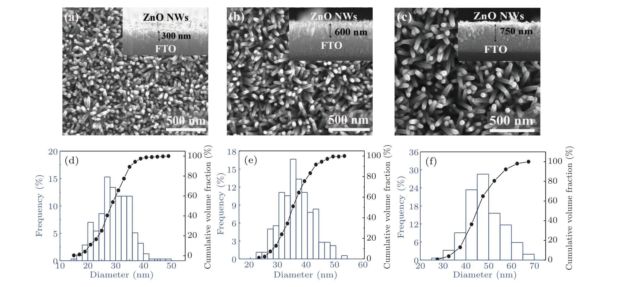
Fig. 3. Top view of SEM images of ZnO NWs for different hydrothermal times. The corresponding cross-sectional images are inserted. The NW diameter distribution and volume fraction cumulative percentages are shown below: (a)and(d)for ZnO1h,(b)and(e)for ZnO2h,(c)and(f)for ZnO3h.
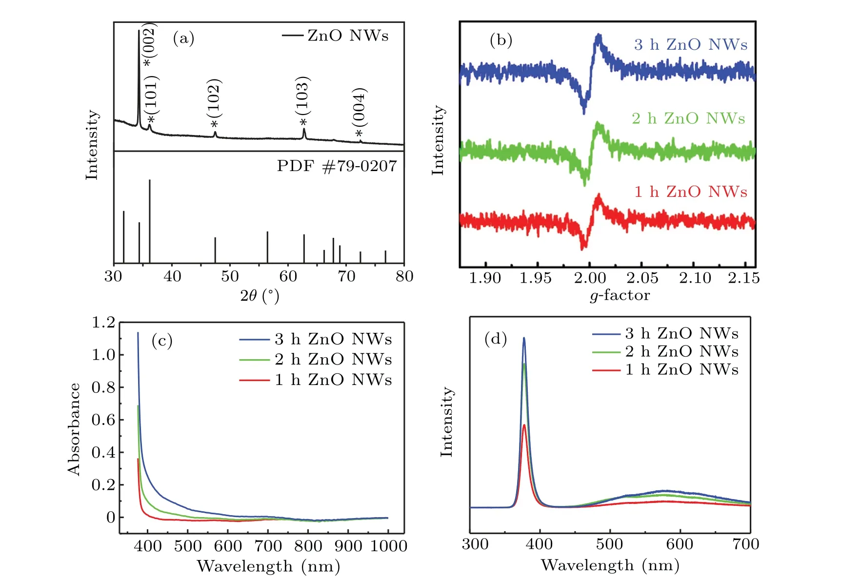
Fig. 4. (a) XRD pattern of ZnO1h NWs. (b) ESR spectra of ZnO NWs with different hydrothermal times. (c) Absorption spectra and (d)photoluminescence spectra of ZnO nanowires for different hydrothermal times.
The prepared ZnO NWs have hexagonal wurtzite structure wherec-axis acts as the polar axis. In this case, oxygen ions are arranged in hexagonal dense packing while Zn ions fill the tetrahedral gap. Half of the tetrahedral gap in the structure is empty,which is easy to produce intrinsic donors of Zn gap defects and O vacancy defects. With prolonging hydrothermal time,the luminescence intensity in UV and visible regions are both enhanced, indicating the increasement of the V+Odefect population. The spectral observations are consistent with the ESR results.
The large amount of defect states greatly enhances the photoelectron generation under visible light excitation,which provides an effective way for the photoreduction of metal ions.Hence,we used blue-ray(403.4 nm,140 mW·cm-2)as the excitation light to investigate photochromism of the Ag+/ZnO1hcomposite system,as shown in Fig.5(a). The absorption spectra for the irradiation times from 0 min to 25 min are obtained. The differential absorption spectra exhibit an effective absorption enhancement covering the whole visible region from 400 nm to 800 nm, which is centered at 405 nm. The band is hard to be found within the initial irradiation period of 3 min, but increases significantly in the subsequent process. A similar result is obtained for the other two samples of Ag+/ZnO2hand Ag+/ZnO3h. We also measured thein situphotoluminescence spectra of Ag+/ZnO1hnanocomposite system under the excitation from a UV laser (325 nm, 35 mW)with different excitation periods (0 min, 5 min and 10 min,respectively), as shown in Fig. 5(b). It can be seen that the UV luminescence intensity of the ZnO loaded with silver ions decreases obviously. Differently, we found that the luminescence ability of ZnO in the visible region(centered at 570 nm)increases slightly after the adsorption of silver ions[Fig.5(b),inserted], which may be related to the localized surface plasmon enhancement.
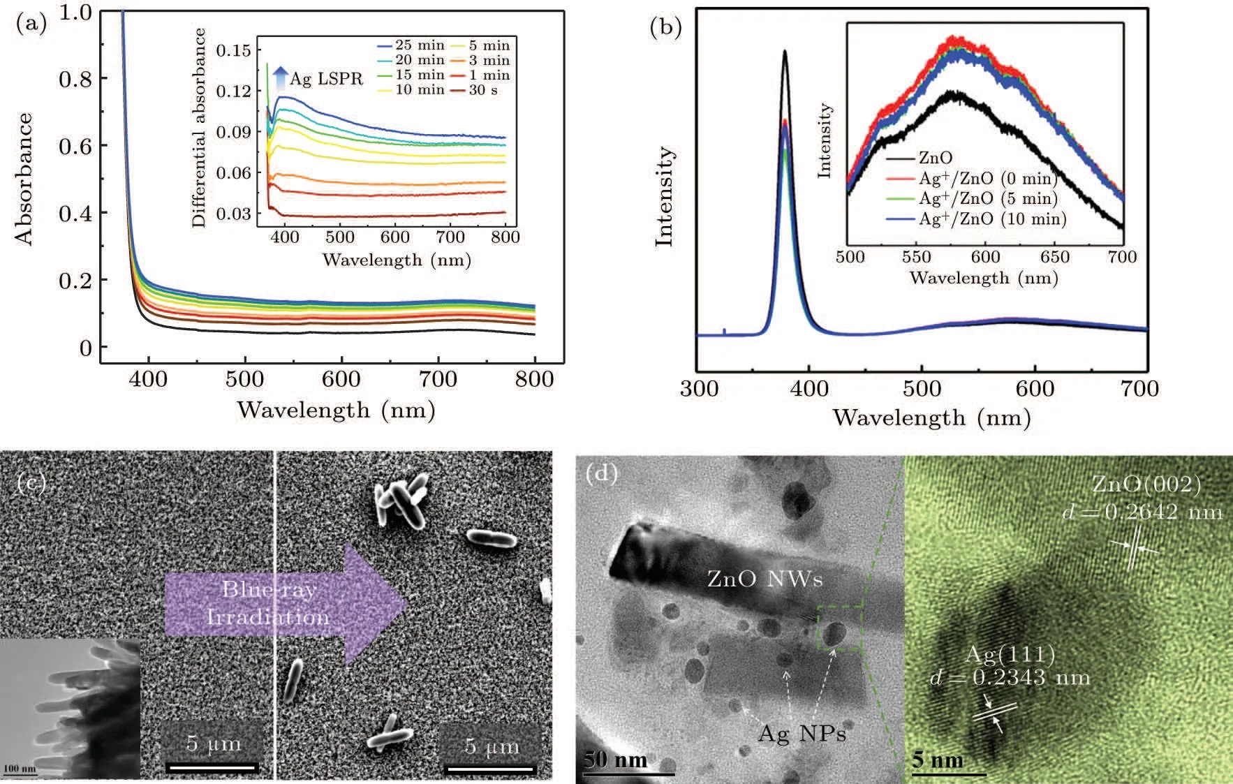
Fig.5.(a)Absorption spectra and differential absorption spectra(inserted)of the Ag/ZnO1h nanocomposite under the 403.4 nm laser irradiation.(b)Photoluminescence spectra of the ZnO1h NWs before and after the treatment of AgNO3 solution,as well as that under 325 nm excitation for different periods (0 min, 5 min and 10 min). The magnification graph in visible region is inserted. (c) Top view of SEM images for the nanocomposite system before and after the blue-ray irradiation. The TEM image is inserted for the ZnO1h NWs without Ag particle deposition.(d)TEM and HRTEM observations for the blue-ray induced emerging of Ag NPs on ZnO NWs via scratching from the prepared Ag/ZnO film.
The absorption and photoluminescence spectral changes in visible region both indicate the possibility of generation of plasmonic particles. Accordingly, surface morphological change was measured byin situSEM for Ag+/ZnO1hbefore and after laser irradiation (140 mW·cm-2), as shown in Fig. 5(c). Before the irradiation, only the ZnO NW surface morphology can be observed, as shown in the inserted graph of Fig. 5(c). After the blue-violet excitation, Ag nanorods appear on the surface of ZnO NWs. The TEM was used to observe the change in the gap of ZnO NWs, as shown in Fig. 5(d). A large amount of spherical Ag nanoparticles(NPs)appear on ZnO NWs with a wide size distribution from 5 nm to 35 nm. High-resolution transmission electron microscopy (HRTEM, the right-side image in Fig. 5(d) proves the nature of the Ag/ZnO contact. The(111)crystal plane of Ag NPs and the (002) crystal plane of ZnO are determined.As ZnO is usually n-type, the Schottky contact may form at the metal-semiconductor interfaces according to our previous investigation.[35]The description equations of photochemical reaction process are expressed as follows:
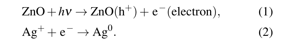
As is known, the electrons at ZnO defect state can absorb photons and jump to the conduction band under the irradiation of the blue-violet light. Ag+ions adsorbed on the surface of ZnO NWs during previous immersion are further photo-reduced. ZnO in exciting state is thus used as an electron donor,and the photogenerated electrons of ZnO interface are transferred to Ag+to generate Ag nucleus. Photochemical reaction is conducted on the surface or in the gap of NW arrays to induce Ag nuclei self-assembly. The regular surface structure of NWs provides convenience for the Ag particle aggregation,which results in large-sized Ag nanorods rather than small spherical NPs. Finally,rod-like Ag NPs emerges on the surface of the NW arrays. However,spherical Ag NPs tend to form in the gap of ZnO NWs due to the limited space. The one-dimensional NW structure has large specific surface area than planar structure,which can provide multiple sites for Ag+loading and form point/line heterojunction. In the reduction process, multiple electron transport channels are provided by sufficient contacting sites, which accelerate the reduction of the Ag+ions adsorbed on the NW surface. The emergence of Ag NPs results in LSPR absorption, which well explains the absorption band in visible region from 400 nm to 800 nm in Fig.5(a). However,in Fig.5(b),under the continuous irradiation of the excitation light source,the UV luminescence intensity decreases firstly(from 0 min to 5 min)and then increases(from 5 min to 10 min). We believe that this process is related to the capture of photogenerated electrons by silver ions and the resultant emergence of Ag NPs. The population decrease of the photoelectrons for recombination with holes results in weakening of intrinsic luminescence. After UV irradiation for 5 min,some silver nuclei are formed and quite amount of silver ions exist. At this time,the Ag+/ZnO nanocomposite system has a strong ability to absorb the 325 nm light energy to generate Ag NPs. When the system is illuminated for 10 min,the content of the resident silver ions decreases significantly,so the light absorption capacity at 325 nm is weakened and the intrinsic emission capacity is partially restored.
The results from Fig. 5 indicate that blue-ray irradiation plays a key role in variation of optical properties of the Ag+/ZnO NWs system. Thus holographic fringes with periodically bright and dark regions can be copied onto such a photosensitive medium. ZnO NWs in the bright area generate photoelectrons for the reduction of Ag+ions; while the medium in the dark area is not irradiated by the laser,and thus maintains its original properties. The Ag0in the bright area and Ag+in the dark area have a sharp contrast in absorbance and refractive index,and the information is thus stored on the sample as a form of interference fringes.The results for testing holographic efficiency are shown in Fig.6.
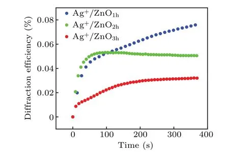
Fig. 6. First-order diffraction efficiency versus time for Ag+/ZnO1h,Ag+/ZnO2h and Ag+/ZnO3h.
The highest diffraction efficiency of Ag+/ZnO1hcomposite film can reach 0.08%. However, the diffraction efficiencies of the other two composite films of Ag+/ZnO2hand Ag+/ZnO3hare lower than that of the Ag+/ZnO1hcomposite system, with the highest diffraction efficiencies reaching 0.05% and 0.03%, respectively. We believe that the diffraction efficiency of the nanocomposite system is related to the factors such as generation efficiency of photoelectrons, loading amount of Ag+ions and light-scattering on sample surface. According to ESR test results,ZnO3hexhibits the largest amount of oxygen defects among the three kinds of samples. Under the same conditions, the number of photogenerated electrons is the largest. The formed holographic gratings should have presented the highest contrast between bright and dark regions. However, the test results show that the composite film of Ag+/ZnO3hhas the lowest diffraction efficiency during the same excitation period. That means that light scattering on the sample surface must be taken into account.When the length of ZnO NWs increases, it is impossible to ensure that each NW grows at the same rate. With the long-term growth of NWs, the surface flatness decreases. The incident light in the bright region can be easily scattered to the dark one,also weakening the grating contrast.At the same time,the amount of Ag+loading sites is insufficient on the surface due to the lowest NW density on the surface of Ag+/ZnO3h. Thus,the lowest diffraction efficiency for Ag+/ZnO3his reasonable.The above results indicate that the Ag+/ZnO nanocomposite system can effectively memorize holographic gratings under visible light excitation in short wavelength region,and the high diffraction efficiency of the Ag+/ZnO1hsample provides possibility for the storage and reconstruction of holographic images. Using red light(671 nm)as the read-out light,the image of the “Eiffel Tower” is stored. Figure 7 shows the original image and its holographic reconstruction at the writing times of 50 s, 100 s and 300 s, respectively. It is worth pointing out that the amount of defects generated in the hydrothermal process is still limited, although the internal defects of ZnO have provided important support for improving the diffraction efficiency of the sample. Towards the application of ultra-fast and high-density holographic storage,the sample performance can be optimized in two aspects: One is introducing impurities or plasma treatment in the ZnO to create more defects so as to expand optical response range and to increase the population of photogenerated electrons. The other is increasing the loading amount of Ag+ions to enhance the reduction reaction,to improve the grating contrast, and to realize more efficient hologram storage.
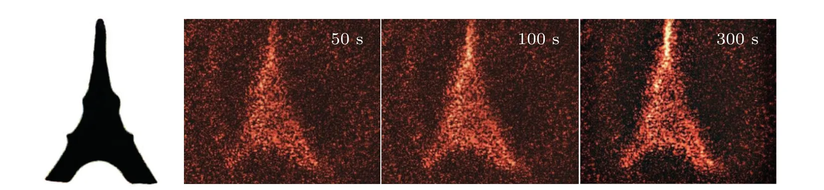
Fig.7. Original image(left,black),and the hologram reconstruction in the Ag+/ZnO1h composite by red light.
4. Conclusion
In summary, an Ag+/ZnO nanocomposite system has been constructed using the hydrothermal-immersion method.The internal oxygen defects in ZnO broaden the light response band, and photogenerated electrons can be effectively generated under blue-violet excitation. The length and the defect content of NWs are dependent on hydrothermal time. Onedimensional nanostructures provide a large number of contacting sites for the subsequent loading of silver ions,forming multiple point/line hetero-interfaces, which are used to transfer photogenerated electrons from the semiconductor side to the silver ions, resulting in the formation of Ag nuclei. In addition, the NW structure provides an excellent growth environment for the formation of Ag nanorods on the array surface.We also compared the effect of NW length on the diffraction efficiency. The results show that the surface of ZnO1hNWs can reduce the light scattering,and improve the light energy utilization.The holographic diffraction efficiency reaches 0.08% for Ag+/ZnO1h. Efficient integration of generation,transmission and storage for optical information is expected to be realized in ZnO-based nano-devices.
Acknowledgements
This work was supported by the National Natural Science Foundation of China(Grant Nos.11974073,U19A2091,and 51732003), the Overseas Expertise Introduction Project for Discipline Innovation (Grant No. B13013), the Natural Science Foundation of Jilin Province of China (Grant No. 20180101218JC), and The 13th Five-Year Scientific Research Planning Project of the Education Department of Jilin Province,China(Grant No.JJKH20201161KJ).

- Chinese Physics B的其它文章
- Surface modulation of halide perovskite films for efficient and stable solar cells
- Graphene-based heterojunction for enhanced photodetectors
- Lithium ion batteries cathode material: V2O5
- A review on 3d transition metal dilute magnetic REIn3 intermetallic compounds
- Charge transfer modification of inverted planar perovskite solar cells by NiOx/Sr:NiOx bilayer hole transport layer
- A low-cost invasive microwave ablation antenna with a directional heating pattern