Intrinsic V vacancy and large magnetoresistance in V1-δSb2 single crystal
2022-03-12 07:45:02YongZhang張勇XinliangHuang黃新亮JingleiZhang張警蕾WenshuaiGao高文帥XiangdeZhu朱相德andLiPi皮靂
Chinese Physics B 2022年3期
Yong Zhang(張勇) Xinliang Huang(黃新亮) Jinglei Zhang(張警蕾)Wenshuai Gao(高文帥) Xiangde Zhu(朱相德) and Li Pi(皮靂)
1Institutes of Physical Science and Information Technology,Anhui University,Hefei 230601,China
2Anhui Province Key Laboratory of Condensed Matter Physics at Extreme Conditions,High Magnetic Field Laboratory of the Chinese Academy of Sciences,Hefei 230031,China
Keywords: binary pnictide semimetals,vanadium vacancy,flat band,weak anti-localization
1. Introduction
Topological insulators have attracted significant attention as they possess helical surface states protected by time reversal symmetry.[1-5]Due to the topological origin and Dirac fermion nature of the topological surface states,the topological insulators are expected to perform excellently in transport behaviors.[6,7]After the discovery of fascinating topological insulators,the binary pnictide semimetalsXPm2(X=V,Nb,Ta;Pm=As,Sb)[8](listed in Table 1)have also become a focus of attention in the field of condensed matter physics. The electronic structures of such materials are protected by an interplay of symmetry and topology. Electronic transport shows many novel quantum phenomena such as large non-saturation magnetoresistance (MR),[9-15]ultrahigh carrier mobility,[16]negativeMR.[17-19]These multifunctional characteristics not only provide us a promising platform for fundamental physical research but also open up a new route for exploring the potential spintronic applications which is one of the most important reasons why these materials have stimulated unprecedented research.[20]
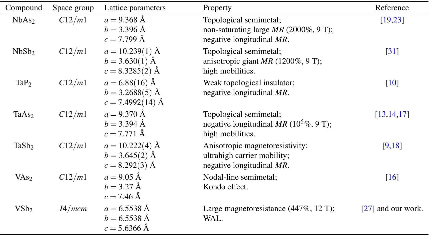
Table 1. Property of binary pnictide semimetals XPm2.
VSb2has long been known as a thermoelectric material.[21]It has been recognized that this type of material is one of the candidates for diffusion barriers or electrodes in thermoelectric devices based on skutterudites.[22]Interestingly, VSb2crystallizes in tetragonal crystal structure, rather than the monoclinic one for other binary pnictides VAs2,[16]NbAs2,[19,23]and TaAs2.[13]So far,there are a few researches on VSb2single crystal.[21]In this work,we successfully grow the large size and high-quality single crystals of V1-δSb2.We systematically characterize its crystal structure, electrical transport, magnetism properties, specific heat, and calculated its band structure.
2. Experimental details
The high-quality V1-δSb2single crystals were synthesized by self-flux method.[24]V dendritic crystals (4N) and Sb(4N)pieces with V:Sb molar ratio of 1:30 were mixed and held in an alumina crucible,and sealed in an evacuated quartz tube. The quartz tube was heated to 1100°C in 10 hours.After holding at this temperature for 20 hours, the tube was slowly cooled to 700°C at a rate of 3°C/h. The tube was then removed from the furnace and inverted into a centrifuge to remove the excess molten antimony. The resulting metallic luster single crystals with several millimeters size were collected from the crucible. The typical dimensions of the V1-δSb2single crystals are 1 mm×1 mm×0.5 mm and show no signs of instability or degradation when exposed to air. The compositions and elemental stoichiometry of the crystals were determined by energy-dispersive spectrometer (EDS) on Oxford X-MAX electron spectrometer equipped on the focused SEM/FIB dual beam system(Helios Nanolab600i,FEI Inc.).
A single crystal was selected and data were collected on a Bruker D8 Quest diffractometer with a detector using a CuKαradiation source(λ=1.54184 °A)from a rotating anode in a range of 10°-90°. Magnetization data were obtained from a Quantum Design magnetic property measurement system(MPMS-7) magnetometer with a 7-T superconducting magnet.The magnetization measurements of V1-δSb2single crystal were performed with zero-field cooling (ZFC) process on MPMS.
Electrode was made by spot welding using 25-μm gold wire, and electrical transport measurements were carried out by the four-probe method upon a physical property measurement system(Quantum Design, PPMS-14T)at a temperature range from 1.8 K to 300 K.During the measurements,a model 372 (AC) resistance bridge and temperature controller were used for the measurement of resistance with applied current of 3.16 mA.The low-temperature specific heat measurements were carried out upon a 16-T physical properties measurement system(Quantum Design,PPMS-16T)using the standard thermal relaxation method.
The preliminary first-principles band structure calculations were performed based on the density functional theory (DFT), and use the projector augmented wave method as implemented in the Viennaab initiosimulations package(VASP).[25]The generalized gradient approximation with the Perdew-Burke-Ernzerhof (PBE)[26]realization was adopted for the exchange-correlation functional. The cutoff energy was set as 400 eV.The energy and force convergence criteria were set to be 106eV and-0.05 eV/°A,respectively.
3. Results and discussion
According to the previous report,[27]CuAl2-type structure V1-δSb2crystallizes in the tetragonalI4/mcmspace group(No.#140). Figures 1(a)and(b)show the crystal structure of V1-δSb2,which can be regarded as alternating stacking layers of V and Sb atoms by ABAB sequence along thecaxis.Each V atom is octahedrally coordinated by Sb atoms with a bond distance of 2.484(8) °A.[28]
Figure 1(c) shows the EDS spectrum for V1-δSb2, the measurements were performed at different positions on the polished surface of the crystal. The average chemical composition ratio of V:Sb was established to be 31.45%:68.55%,which confirms the existence of V atoms vacancies in the V1-δSb2single crystal withδ ≈0.08. This value is approximately in accordance with previous phase diagram studies(V0.9Sb2[29]and V0.97Sb2[21,22]). This means that V1-δSb2phase with V vacancy is more stable at ambient pressure,while VSb2with the same space groupC12/m1 as NbAs2may be stabilized under high pressure.
Figure 1(d)shows the single crystal XRD pattern for the V1-δSb2at room temperature. Two sharp diffraction peaks that represent (00l) plane can be observed. The inset shows the rocking curve of the(002)diffraction peak,the full width at half-maximum(FWHM)is estimated to be Δθ ≈0.05°. Such a narrow FWHM indicates the high quality of the single crystal without twin crystal.
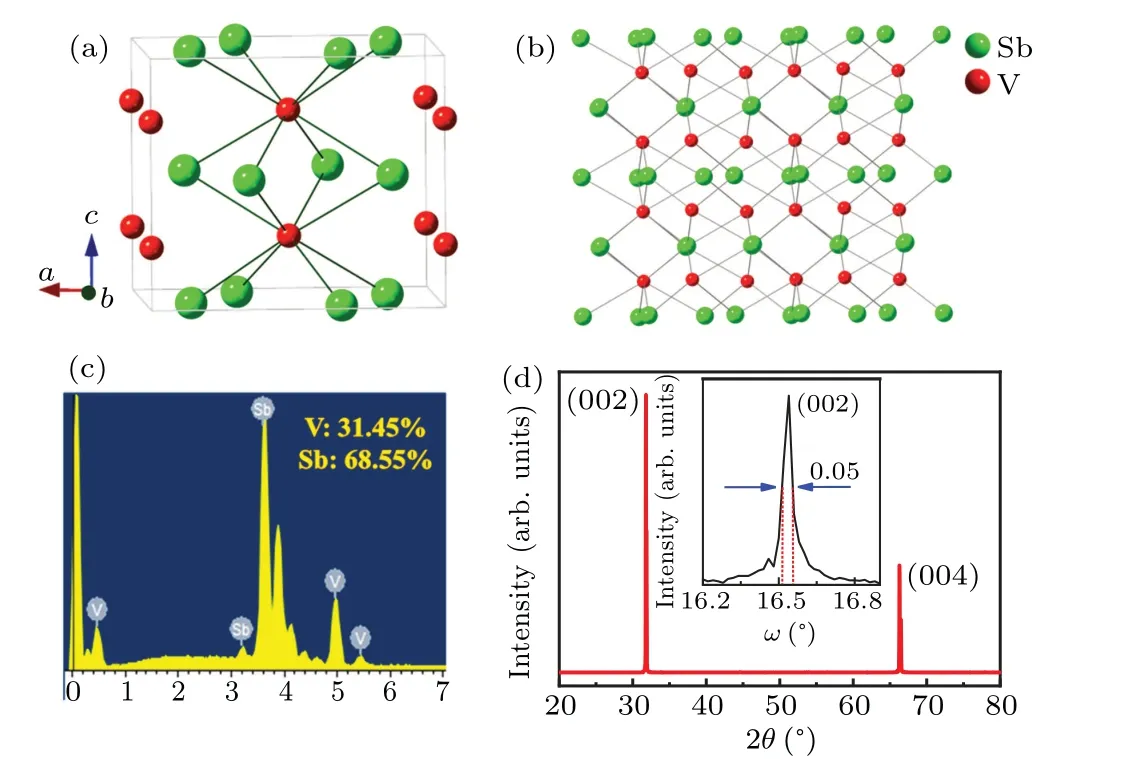
Fig. 1. (a) and (b) Crystal structure of the V1-δ Sb2 single crystal. The red sphere represents vanadium atoms,the green sphere represents antimony atoms.(c)The topical energy dispersive spectrometer(EDS)for single crystal V1-δ Sb2. (d) X-ray diffraction pattern of V1-δ Sb2 single crystal with the corresponding Miller indices (00L) in parentheses. The inset shows a corresponding rocking curve.

Fig.2. (a)The temperature dependence of longitudinal ρxx from 1.8 K to 300 K at the zero magnetic field. The value of RRR is 10.7. Upper inset shows a photograph of V1-δ Sb2 single crystal on millimeter-grid paper. (b)The ρxx at different magnetic fields. (c)The normalized MR at temperature ranging from 1.8 K to 300 K.
Figure 2(a) exhibits the temperature dependence of longitudinal resistivityρxxfor V1-δSb2single crystal in the temperature range of 300 K-1.8 K without magnetic field. The inset displays the typical view of a V1-δSb2single crystal placed on a millimeter grid with the preferential orientation along the[001]zone axis. The residual resistance ratio(RRR),RRR=ρxx(300 K)/ρxx(2 K)=10.8, is relatively lower than that of VAs2(12),[16]NbAs2(150),[23]and NbSb2(~200).[30]This value is still larger than the reported value of~3.0 in Ref. [22]. Such relatively low value ofRRRfor V1-δSb2should origin from the intrinsic V vacancy,which provides additional scattering centers.
When the temperature decreases from 300 K to 1.8 K,theρxxexhibits metallic behavior. Figure 2(b)plots the temperature dependence of resistivity under different magnetic fields.The electric current is parallel to thebaxis,and the magnetic field is perpendicular to theabplane. When a magnetic field is applied to the V1-δSb2single crystal, theρxxcurves are enhanced obviously with increased magnetic and another important fact observed is thatρxx(T) also increases 18.2% at 12 T at room temperature (300 K). Moreover, the V1-δSb2still holds metallic behavior even at high field of 12 T without any sign of metal-insulator transition,which is quite different from the observation of insulator-like behavior in other binary pnictide semimetals.[12,13,30-32]
Figure 2(c)shows the normalizedMRcurves measured at different temperatures and the magnetic field is applied perpendicular to the(001)plane. TheMRis defined as

Hereρxx(H) andρxx(0) are longitudinal resistivities with and without magnetic field,respectively. The normalizedMRcurves are symmetrized viaMR(B)=[MR(B)+MR(-B)]/2 to remove the contribution of Hall resistance. AtT=1.8 K,V1-δSb2single crystal exhibits a largeMRof 447% atB=12 T.With the increase of temperature,MRis suppressed significantly but still remain about 18.2%at 300 K.The classical carrier compensation mechanism was used to explain the large and non-saturating quadraticMR, such as that of in WP2[33]and Nb3Sb.[34]Based on the band structure calculation in Fig. 5, although we observed the electron and hole pockets fromΓtoXpoint, such a mechanism seemed to be invalid because the field dependence ofMRin V1-δSb2single crystal was of significant deviation from quadratic behavior. On the other hand, similar largeMRbehavior had been observed in nonmagnetic half-Heusler ScPtBi single crystals.[35]Therefore,the largeMRfor V1-δSb2single crystal could be understood as the WAL effect makes resistance increase steeply near zero fields. Remarkably, we observed that theMRincreases sharply in the low field region under 20 K, and a largeMRof 180% is obtained in a magnetic field of 1 T at 1.8 K. TheMRin V1-δSb2single crystal is much larger than many other nonmagnetic compounds,such as ScPdBi,[36]LuPtSb,[37]and Bi2Te3.[38]This distinctMRdip near zero magnetic field can be associated with the weak antilocalization (WAL) effect.The WAL effect is generally expected to originate from the topologically protected surface state,[39-41]or strong spinorbit coupling.[42]At zero magnetic field,backscattering gains the minimum due to the time-reversal symmetry. As the magnetic field increases,the time-reversal symmetry is broken and the backscattering increases, which leads to a sharp increase ofMR. It has been widely observed in topological insulators (Bi-Se-Te[43-45]) and topological superconductors (Al-InAs[46]and LuPdBi[47]). Furthermore, such phenomenon has also been reported in systems with strong spin-orbit couplings,such as LuPtSb[37]and YPdBi.[48]
In order to deeply understand the WAL effect in V1-δSb2single crystal, we fit the corresponding magnetoconductivity Δσxx(B) =σxx(B)-σxx(0) using the Hikami-Larkin-Nagaoka(HLN)formula[49]
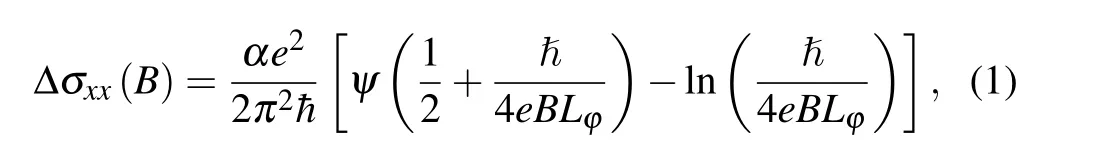
whereeand ˉhare electron charge and reduced Planck constant;ψis digamma function;αandLφare the prefactor and phase coherence length, respectively. The prefactorαdenotes the number of conduction channels, which is experimentally found to be-0.5 for each conductive channel in two-dimensional (2D) topological insulator. Figure 3(a) displays the low-field magnetoconductivity Δσxx(B)from-0.3 T to 0.3 T at temperatures ranging from 1.8 K to 20 K, and all the curves can be well fitted by the HLN model. The obtained phase coherence lengthLφas a function of temperature are shown in Figure 3(b), and the inset displays the temperature dependence of parametersα. Remarkably, the value ofαwith an order of 105is larger than the theoretical 2D electron system, hinting that the WAL effect is mainly originate from the strong spin-orbit coupling of the three-dimensional(3D) bulk state in the V1-δSb2single crystal. In addition,we measure the angle-dependent Δσxx(B)at 1.8 K under low magnetic fields from-1 T to 1 T, as shown in Fig. 3(c). In the 2D topological insulator, the Δσxx versus Bsinθcurves should converge to one curve. The Δσxx versus Bsinθcurves in V1-δSb2are separate from each other, which further confirms the 3D feature of the WAL effect. All the results reveal that the WAL effect in V1-δSb2is resulted from strong spin-orbit coupling (SOC) destructive quantum interference between time-reversed loops formed by scattering trajectories,leading to the conductivity enhanced with decreasing temperature in the 3D bulk transport.[41]
Fig.3. (a)The normalized magnetoconductance(Δσxx)at different temperatures(color hollow circle)and the black line is corresponding fitting curve.(b)Temperature dependence of the fitting parameter Lφ phase coherence length deduced from the WAL fit. The inset shows the temperature dependence of α. (c) The Δσxx plotted in the perpendicular magnetic field component of the magnetic field, Bsinθ, at 1.8 K. Inset, schematic diagram of the measurement setup where θ indicates the angle between the direction of the magnetic field and(001)plane.
In addition,we measured the anisotropic magnetic properties of the V1-δSb2single crystal. Figure 4(a) shows the magnetic susceptibilityχ-Tcurve with applied magnetic field parallel and perpendicular to(001)plane,respectively. Obviously, the temperature-dependent paramagnetic susceptibility curves show typical paramagnetic behavior with nonnegligible anisotropic, and theχcis relatively larger thanχab. Both curves can be well fitted with the Curie-Weiss lawχ=χ0+C/(T-θ),[50]whereχ0is the temperature-dependent paramagnetic susceptibility from the electron contribution near the Fermi level,Cis Curie constant,θis the Weiss temperature.For both curves, the determinedCandθare almost identical with the values of about 0.0174(9) emu·mol-1·Oe-1·K-1(1 Oe=79.5775 A/m)and-183.7(3)K,respectively. The effective momentum was determined to be 0.3741μB/V atom.The negativeθvalue indicates the existence of antiferromagnetic coupling between V atoms or vacancy. By subtracting the Curie-Weiss part,theχ0part can be obtained and is shown in the inset of Fig. 4(a). Apparently,χ0forH||cremains in whole temperature range down to 4 K with a small curie tail,whileχ0forH||abstarts to increase suddenly with decreasing temperature below 15 K.Such a sudden increase ofχ0forH||abmay not come from magnetic order, since the antiferromagnetic coupling. Figure 4(b) shows the typical paramagnetic behaviors forH||c,and the magnetization is extremely small at 2 K,which confirmed that an abrupt increase of theχ0part is not induced by the magnetic order.On the other hand,if we attribute the abrupt magnetization increment ΔMbetween 2 K and 20 K(3.4×10⁻²emu·mol-1)to the ferromagnetic impurity,we can obtain a concentration with 10-6order for magnetic impurity. In classic condensed matter physics, theχ0is proportional to the density of Fermi level with small magnetic fieldHwith relation of[51]
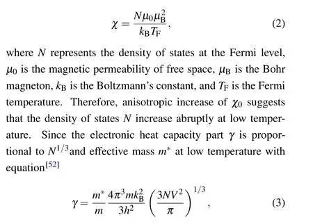
wheremis the mass of free electrons,his the Planck constant,Vis the volume per mole. Theoretically,an abrupt increase ofNat low temperature is expected to yield an abrupt increase ofγin specific heat.
Heat capacity was measured between 2 K to 10 K and no phase transition was observed. The total heat capacity of normal metal material at low temperature can be described as the sum ofC=Ce+Cp=γT+βT3,[52]whereCpis the phonon contribution,γandβare the free electron part coefficient and phonon part coefficient. To obtain theγpart,C/T versus T2curve is plotted in Fig. 4(c). By linear fitting of the curve,phonon part coefficientβ= 0.16529 mJ·mol-1·K-4can be obtained. As shown in Fig. 4(c), theC/T-T2deviates from the simple model for a normal metal below 7 K.As mentioned above, the estimated low concentration of ferromagnetic impurity is of 10-6order, which cannot explain the heat capacity change below 7 K. After subtracting the phonon part, the temperature dependence ofγcan be obtained,as displayed in Fig. 4(d). We propose that theγfree electron part suddenly increases under 7 K,which means that the abrupt increase ofγinduced by the abrupt increase ofNat low temperature. To figure out the physics origin,band structure calculations were made.
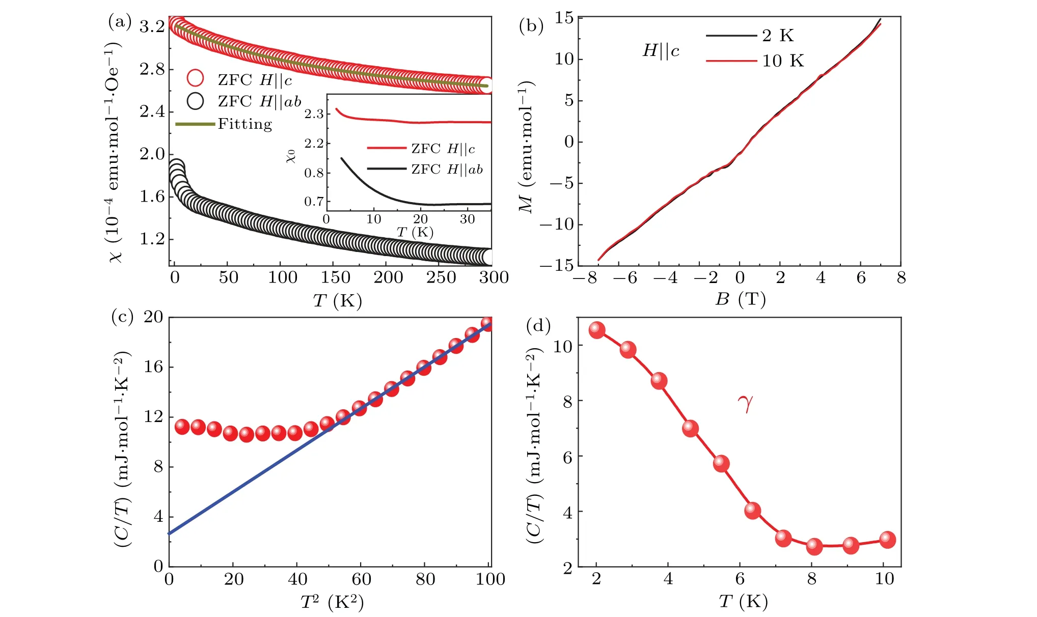
Fig.4. (a)The magnetic susceptibility of V1-δ Sb2 single crystal with under zero field cooling(ZFC)for field of 0.2 T applied parallel to c axis and perpendicular to ab plane. The brown line is fitting with the Curie-Weiss law and the inset shows a temperature-dependent paramagnetic susceptibility gained by magnetic susceptibility subtracted the Curie-Weiss part. (b)Field-dependent magnetization at 2 K,10 K,respectively.(c)C(T)/T versus T2 of V1-δ Sb2 single crystal from 2 K to 10 K.(d)The free electron part coefficient γ(C/T-βT2)versus temperature T,where β is determined from the linear fitting(blue solid line).
Fig.5. (a)The Brillouin zones. (b)Band structures calculated with considering spin-orbit coupling(SOC)and the total density of states(DOS)for VSb2.(c)The Fermi surfaces of VSb2 crystals from first-principle calculations. Left is total Fermi surface for VSb2,right is Fermi surface with along Γ-X.
We first calculated the band structures with SOC.The obtained results are plotted in Fig.5(b). Then,the Fermi surface was calculated by the VASPKIT.[25]The software of XcrySDen was used to plot the Fermi surface in Fig. 5(c). Figure 5(a) shows the first Brillouin zone in momentum space for the primitive unit cell. The metallic character can be shown by the high density of states (DOS) at the Fermi level and the presence of electron and hole-bands. The DOS of VSb2shows that the region close to Fermi level is dominated by fully occupied V-3d states with a small contribution of Sb-3p states and that conduction bands are dominated strongly by this hybridization.[27]The left of Fig.5(c)reveals the total Fermi surface include the six bands crossing Fermi level. The right picture shows a flat band, that crosses the Fermi surface alongΓ-Xpoint,consists of hole-and electronpockets. The electron-pocket encompasses theΓpoint. The hole-pockets, located on theXpoint, which is in the center of the hexagonal plane of Brillouin zone. According to the previous research, from 300 K to 10 K, V0.97Sb2single crystal has a relatively large linear coefficient of thermal expansionα1= 14.1×10⁻⁶K-1, which value is higher than the reported value for NbSb2(8.4×10⁻⁶K-1) and TaSb2(7.5×10⁻⁶K-1).[22]With the decrease of temperature, the structure of V1-δSb2single crystal is distorted and the flat band gradually approached the Fermi surface. When the temperature falls below 7 K, the flat band is closer to the Fermi surface and produces a large density of states. This is the reason why the magnetic susceptibility and theCeincrease at low temperatures.
4. Conclusions
High-quality V1-δSb2single crystals were grown via flux method. Due to VSb2possesses a narrow homogeneity range,the vanadium compound possesses a V deficiency and is better described as V1-δSb2(δ ≈0.08).We have calculated the electronic structure with SOC and measured the longitudinal resistivity, specific heat, and magnetic susceptibility of V1-δSb2.Transport experiments demonstrated that V1-δSb2performs metallic behavior with positive largeMRreached 447%. More intriguingly, we observed an obvious WAL effect fromMRbelow 20 K in the low-field region. The extremely largeαand the angle dependence of Δσxxsuggest that the WAL effect in V1-δSb2single-crystal originates from the contribution of strong 3D bulk spin-orbital coupling. In addition, we observed the abruptly increase of theχ0part andCepart under the 7 K.We propose that these phenomena are signatures of the flat band, which indicates V1-δSb2is likely to display fantastic electronic behaviors at extremely low temperatures.
Acknowledgements
Project supported by the National Natural Science Foundation of China (Grant Nos. U2032214, U2032163, and 11904002), the Youth Innovation Promotion Association of Chinese Academy of Sciences (Grant No. 2017483), and the Natural Science Foundation of Anhui Province,China(Grant No.1908085QA15).
- Chinese Physics B的其它文章
- Surface modulation of halide perovskite films for efficient and stable solar cells
- Graphene-based heterojunction for enhanced photodetectors
- Lithium ion batteries cathode material: V2O5
- A review on 3d transition metal dilute magnetic REIn3 intermetallic compounds
- Charge transfer modification of inverted planar perovskite solar cells by NiOx/Sr:NiOx bilayer hole transport layer
- A low-cost invasive microwave ablation antenna with a directional heating pattern