Magnetoresistance effect in vertical NiFe/graphene/NiFe junctions
2022-03-12 07:44:54PeiSenLi李裴森JunPingPeng彭俊平YueGuoHu胡悅國YanRuiGuo郭顏瑞WeiChengQiu邱偉成RuiNanWu吳瑞楠MengChunPan潘孟春JiaFeiHu胡佳飛DiXiangChen陳棣湘andQiZhang張琦
Chinese Physics B 2022年3期
Pei-Sen Li(李裴森), Jun-Ping Peng(彭俊平), Yue-Guo Hu(胡悅國), Yan-Rui Guo(郭顏瑞),Wei-Cheng Qiu(邱偉成), Rui-Nan Wu(吳瑞楠), Meng-Chun Pan(潘孟春),Jia-Fei Hu(胡佳飛), Di-Xiang Chen(陳棣湘), and Qi Zhang(張琦)
College of Intelligence Science and Technology,National University of Defense Technology,Changsha 410073,China
Keywords: magnetoresistance effect,graphene,magnetic junctions,spintronics
1. Introduction
As one of the primary spintronic devices, the magnetic tunnel junction (MTJ) consisting of an insulating barrier between two metallic ferromagnetic (FM) layers has many applications, such as magnetic field sensors, magnetic random access memories(MRAM),microwave devices,spin logic circuits,etc.[1-7]The magnetizations in two FM layers are decoupled by the barrier layer and are able to switch independently from each other. Driven by the applied magnetic field,the different relative orientations of the magnetizations correspond to diverse resistance values, thus realizing the sensing and detection of external magnetic fields.[8,9]In order to improve the signal-to-noise ratio and reduce the power consumption, the barrier layer is usually required to be as thin as possible while still maintaining a large tunneling magnetoresistance(TMR).This is difficult for the traditional barrier materials such as Al2O3and MgO,because there always exist several problems like pinholes,trap states and defects in these metal oxides, which can induce the shot noise and seriously compromise the performance of MTJs. Meanwhile,the experimental TMR ratio of this kind of MTJ has reached closely to the level of its theoretical value and is extremely hard to make any further breakthrough.[10]Hence, it is now an urgent demand to seek for a new material with excellent properties for the current applications of MTJs.
Graphene, a two-dimensional (2D) honeycomb material of carbon atoms, has aroused much interest due to the superior properties since its discovery.[11-14]The high in-plane carrier mobility and low spin-orbit coupling in graphene can create long spin lifetimes and diffusion lengths, enabling the realizing of lateral spin devices with novel features and functions.[15-19]On the contrary, the weak out-of-plane conductivity of this atomically thin material makes it an effective insulator for the transport perpendicular to the plane,thus providing an alternative choice for the barrier material of MTJs.[20,21]Encouragingly, as expected, it has been theoretically predicted that the graphene-based MTJ has an extraordinarily large TMR ratio due to its almost perfect spin filtering effect atKpoint at the graphene/FM interface.[22,23]Provided that this prediction comes true, it will be significantly beneficial to the application of MTJs. Given this, a variety of graphene-based MTJs with current-perpendicularto-the-plane (CPP) geometry have been successively realized experimentally.[20,24-30]
Nowadays,the interface between the graphene interlayer and the bottom FM layer is formed mainly by transferring graphene (grown through chemical vapor deposition (CVD)or mechanically exfoliated from graphite flake) onto the bottom electrode.[20,24-26]It is almost inevitable to introduce the oxidation and contamination into the graphene/FM interface because the bottom electrode is exposed to air in the fabrication process and this impure interface may induce the spin-flip scattering. To this end, some novel schemes were put forward. For example, (i) a suspended graphene membrane is made over a hole,followed by depositing ferromagnetic metals on both sides of graphene; (ii) a graphene layer directly grows on the top of the bottom FM layer.[27-30]However,the experimentally observed TMR ratio was improved merely to a small extent with the value much less than the predicted value,whereas the fabrication procedure became more complicated,which is likely to introduce new potential problems. As an example, the‘Mexican hat’shape of the suspended graphene can form after the FM layer has been deposited and the induced strain locally affects the atomic-scale contact between graphene and FM layers.[28]Besides, there still exist several questions and issues about the growth mechanism of graphene on FM transition metals, and arduous efforts are still needed to improve the graphene quality.[31]Back to the transferring method:the exfoliated graphene usually has a high quality but its size is limited to dozens of microns, which is not scalable for application, so wet transfer of CVD graphene is still the most simple and practical approach. On the other hand, the permalloy(or NiFe),as one of the ferromagnetic materials,is commonly used as the FM electrode of MTJs for the following two merits. Firstly, it has a relatively high spin polarization, which is beneficial to a large TMR ratio. Secondly, the NiFe film has a low coercivity, which is an extremely important property for its application in sensors. According to these considerations, we chose the NiFe film as the FM electrode material. Although the wet transfer method has been reported for fabricating NiFe/graphene/NiFe vertical junctions,[24,25]the anisotropic magnetoresistance (AMR) contribution to the magnetoresistance(MR)effect was not studied. According to the early report,a significant AMR signal was observed in the NiFe/graphene/NiFe devices with exfoliated graphene,[32]so it must be excluded by some powerful experimental evidences.
In this work, we demonstrate the evident MR effect in MTJs consisting of a single layer of graphene between two NiFe electrodes in a relatively simple manner by transferring CVD graphene onto the bottom FM electrode. Meanwhile,the MR ratio dependence on the magnetic field direction is obtained and validates that the origin of MR effect in our devices is not the AMR. The MR curve shows two resistance states hinging on the magnetization alignment configuration between two FM electrodes, with an MR ratio of 0.17% at room temperature. As the bias current increases, the MR magnitude manifests a typical monotonic downward trend,which further excludes the contribution from AMR. In addition, it is found that the current-voltage(I-V)characteristic shows a linear behavior,which indicates the ohmic contacts at the interfaces and the metallic transport behavior of vertical graphene junctions.
2. Fabrication and characterization
For the purpose of rapidly constructing the graphenebased MTJ to demonstrate its MR effect, we chose the approach to directly transferring graphene onto the bottom electrode. In addition, as the mechanical exfoliation process of graphite generally involves tedious identification and positioning of the graphene flakes, the CVD grown graphene on the copper foil was selected as the barrier interlayer in this work,which is also conducive to realizing the wafer-scale fabrication of MTJ devices.
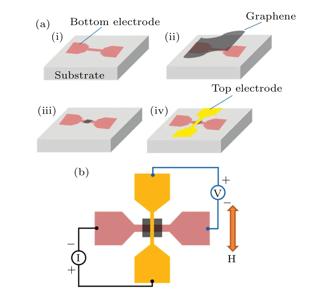
Fig.1. (a)Fabrication procedure of MTJ sample,showing(i)NiFe(30 nm)thin film deposition for the bottom electrode, (ii) transferring CVD grown graphene onto bottom electrode, (iii) patterning graphene by O2 plasma etching, and (iv) NiFe (50 nm) thin film deposition for top electrode. (b)Schematical measurement configuration of MTJ sample.
Figure 1(a) shows that the sample fabrication process of the MTJs in detail.Prior to graphene transfer,the bottom electrode stripes were prepared on an SiO2/Si substrate in which the SiO2layer is 300-nm thick, by using the UV lithography and e-beam evaporation. Specifically, an NiFe thin film with a thickness of 30 nm was deposited on a photoresist-patterned substrate at a 1-°A/s rate, and then the patterned bottom electrode was obtained by using a standard lift-off technique.Subsequently,graphene on the copper foil was transferred onto the bottom NiFe film with assistance of polymethyl methacrylate(PMMA) which had been spin-coated on graphene to serve as the supporting layer. The details of the wet transfer process are as follows. 1)The copper foil was dissolved by etching in the CuSO4/HCl mixed solution and then the PMMA with graphene was rinsed in deionized water several times.2) We transferred the graphene/PMMA bilayer to the target substrate and let it dry naturally in order to increase the adhesion. 3)The PMMA was removed by soaking in the hot acetone. The next step was to remove the unnecessary graphene apart from the position of junctions by 3-min O2plasma etching with a power of 200 W. After that, the 50-nm-thick top NiFe electrode was fabricated by using a similar process to that used for fabricating the bottom electrode. The only difference was that we used the e-beam lithography rather than the UV lithography in view of the extremely narrow top NiFe stripe.Finally,the Ti(50 nm)/Au(70 nm)contact electrode was deposited through e-beam evaporation, thus forming a fourprobe structure. The measurement configuration of MTJs is schematically displayed in Fig.1(b). When the current flowed from the top electrode to the bottom electrode,the corresponding voltage between the two electrodes was measured at the same time. The external magnetic field(0°)was applied along the long axial direction of the top electrode. It is worthy to point out that as the width of the bottom electrode is much larger than that of the top one,it is easier for magnetization in the bottom FM layer to switch under the applied magnetic field due to the weaker shape anisotropy,thus realizing the different switching fields of the two FM layers.
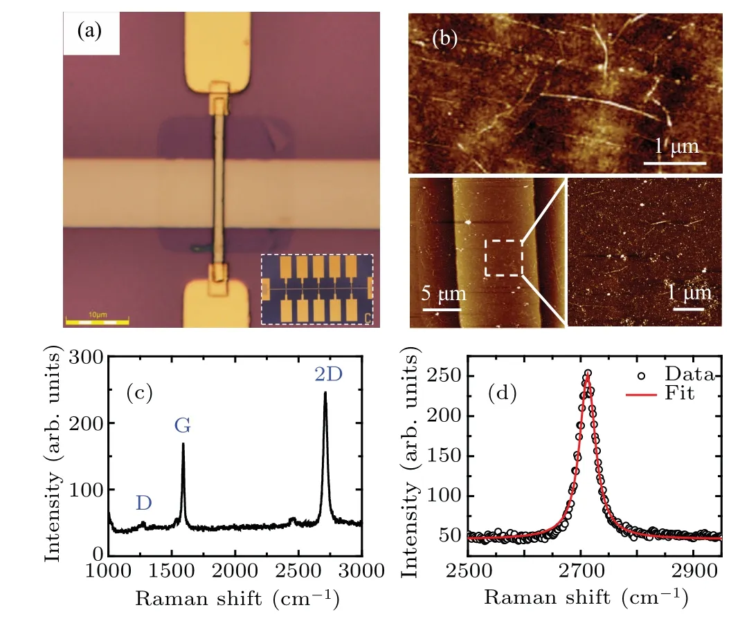
Fig. 2. Characterization results of fabricated MTJs. (a) Optical image of typical MTJ,with inset displaying MTJ array taken by optical microscopy.(b) AFM image of graphene before transfer (upper one) and AFM images after transfer(lower two),of which the lower right one is the magnified image of the dotted box region in the lower left one. (c) Raman spectrum of transferred graphene. (d) 2D band of graphene and its single Lorentzian fitting peak.
Figure 2 indicates a series of characterization measures to estimate the quality of our samples during and after the fabrication. Figure 2(a) shows an MTJ picture taken by optical microscope. The inset displays a top-view optical photograph of the final MTJ array. As shown in Fig.2(b),the atomic force microscopy (AFM) was used to evaluate the cleanliness and flatness of graphene in the transferring process. The upper one and lower two are the AFM images of graphene before and after being transferred onto the bottom electrode stripe,respectively. It can be clearly seen that the graphene cleanliness was basically maintained without any obvious polymer residue. Meanwhile, in order to characterize the thickness and quality of graphene, the Raman spectrum was obtained with a laser excitation wavelength of 532 nm from the transferred graphene as shown in Figs.2(c)and 2(d). Based on the fact that the intensity of 2D (2700 cm-1) peak is larger than that of the G (1590 cm-1) peak and the symmetric 2D band can be fitted into a perfect single Lorentzian peak, it is concluded that the graphene monolayer exists on the bottom NiFe electrode.[33,34]Additionally, no obvious D peak is observed,implying that reasonably high-quality graphene after transfer was obtained,since its intensity reflects the number of defects.
3. Results and discussion
After verifying the feasibility of the fabrication method mentioned above,we prepare numerous MTJ samples and investigate their transport behaviors. As seen in Fig. 3(a), the resistance as a function of the magnetic field (R-Hcurve) is obtained with a bias current of 500 μA at room temperature.It presents two prominent resistance states (parallel and antiparallel)under a sweeping magnetic field along the long axial direction of top electrode (defined as 0°), demonstrating the existence of MR effect in graphene-based MTJs. The switching fields of the bottom and top NiFe electrode can be identified to be about 20 Oe(1 Oe=79.5775 A/m)and 50 Oe. An MR ratio of 0.17% at room temperature is clearly observed by using the MR calculation formulaMR=(RAP-Rp)/Rp,whereRAPandRpare parallel and anti-parallel resistance,respectively. Assuming the spin polarizations (P) of two FM electrodes are the same, we can calculate the value ofPto be 2.9%by adopting the Julliere’s formulaMR=2P1P2/(1-P1P2).What figure 3(b)shows is theR-Hcurve when the magnetic field is applied along the 90°direction(perpendicular to the long axial direction of top electrode). Like in the case of 0°direction,it also manifests the distinct resistance switching.Note that the magnetization reversing is accompanied with a gradual rotation process, which can be attributed to the demagnetizing field caused by shape anisotropy of the magnetic film. The identical positive MR ratio for these two cases validates that the origin of MR effect in our device is not from the AMR. As for the current-voltage characteristic, theI-Vcurve in Fig. 3(c) exhibits a linearly changing trend, revealing the metallic transport behavior of graphene-based MTJs.This is in consistence with most of the recent experimental results.[24-26,28-30]As previously reported, it is believed that there exists a strong hybridization between theπorbitals of graphene and the metal d states of FM electrode,which gives rise to the formation of the hybridization-induced electronic states of graphene around the Fermi energy.[35]This is the key factor resulting in the ohmic contact and metallic transport behavior in our devices. Although the nonlinearI-Vcurve has been discovered in some graphene-based MTJ devices before,it is commonly believed that this originates from the influence of bottom electrode oxidation and contamination residues.[28]Finally,we measure the AMR effect of the bottom NiFe electrode and the related results are shown in Fig. 3(d). As we can see, the resistance of the bottom electrode is much larger than that of the junction and theR-Hcurve is also exceedingly different,which further verifies the results credibility of our devices.
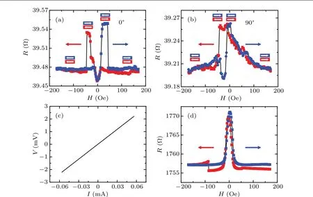
Fig.3. Transport measurement results of MTJ sample. Typical R-H curve at room temperature with 500-μA bias current when the magnetic field is swept along(a)0° and(b)90° directions. (c)I-V curve at room temperature under zero magnetic field. (d)AMR effect measurement of bottom NiFe electrode,with red(blue)arrows indicating corresponding magnetic field sweeping from a positive(negative)maximum to a negative(positive)maximum.
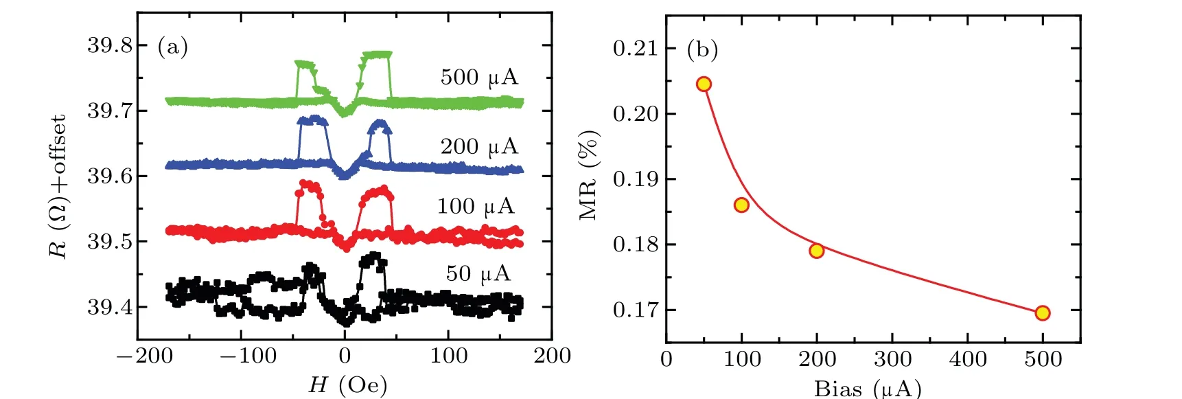
Fig.4. (a)The R-H curves of MTJ sample under different bias currents,which are shifted with a fixed offset;(b)bias dependence of the MR ratio.
Furthermore,in order to reveal the magnetoresistance dependence on the bias, the transport measurements under different bias currents are carried on at room temperature and the related results are displayed in Figs.4(a)and 4(b). For a better display, we add a constant offset among the fourR-Hcurves in Fig.4(a). It is obvious that the MR ratio depends strongly on the bias and manifests a monotonic downward trend as the bias current increases. This is a typical phenomenon for the tunneling magnetoresistance and has been predicted to occur in a wide variety of MTJs.[36,37]It is believed to arise from the interface states and barrier height changed by the bias,which has been theoretically studied in the Ni/graphene/Ni MTJ.[38]In addition,it should be pointed out that this bias dependence of the magnetoresistance is also an powerful evidence for excluding the contribution from AMR that increases with the bias increasing.
4. Conclusions
In this work, a vertical NiFe/graphene/NiFe junction is fabricated in a simple and easy way by transferring the CVD grown monolayer graphene onto the bottom FM electrode.Through the spin transport measurement under a in-plane sweeping magnetic field,the MR effect in the graphene-based junction is demonstrated experimentally, manifesting the distinct high and low resistance states. An MR ratio of 0.17%with a corresponding spin polarization of 2.9%is obtained at room temperature. In order to exclude the contribution from AMR, the magnetic field direction dependence of MR ratio is obtained and shows an identical positive MR ratio for the 0°and 90°directions. Moreover,the MR magnitude depends strongly on the bias and displays a typical monotonic downward trend with the bias current increasing,which further validates that the MR effect in our device is not from the AMR.In addition,the linearI-Vcharacteristic verifies that graphene works not as a tunnel barrier but as a conducting layer, and the transport property in graphene vertical junctions is metallic. Our work is beneficial to further understanding the spin transport behavior in graphene spintronic devices and can also provide a template for fabricating the analogous nano-devices based on 2D materials.
Acknowledgements
Project supported by the National Natural Science Foundation of China (Grant No. 62004223) and the Open Research Fund Program of the State Key Laboratory of Low-Dimensional Quantum Physics,China(Grant No.KF202012).

- Chinese Physics B的其它文章
- Surface modulation of halide perovskite films for efficient and stable solar cells
- Graphene-based heterojunction for enhanced photodetectors
- Lithium ion batteries cathode material: V2O5
- A review on 3d transition metal dilute magnetic REIn3 intermetallic compounds
- Charge transfer modification of inverted planar perovskite solar cells by NiOx/Sr:NiOx bilayer hole transport layer
- A low-cost invasive microwave ablation antenna with a directional heating pattern