
Simulation design of normally-off AlGaN/GaN high-electron-mobility transistors with p-GaN Schottky hybrid gate
2022-06-29 08:56:40YunLongHe何云龍FangZhang張方KaiLiu劉凱YueHuaHong洪悅華XueFengZheng鄭雪峰ChongWang王沖XiaoHuaMa馬曉華andYueHao郝躍
Chinese Physics B 2022年6期
Yun-Long He(何云龍), Fang Zhang(張方), Kai Liu(劉凱), Yue-Hua Hong(洪悅華), Xue-Feng Zheng(鄭雪峰),Chong Wang(王沖), Xiao-Hua Ma(馬曉華), and Yue Hao(郝躍)
Key Laboratory of Wide Band Gap Semiconductor Materials and Devices,School of Microelectronics,Xidian University,Xi’an 710071,China
Keywords: normally-off high-electron-mobility transistor,AlGaN/GaN,p-GaN
1. Introduction
AlGaN/GaN-based HEMTs play an increasingly important role in the field of microwave power due to its high breakdown voltage, high electron concentration and high electron mobility.[1–3]Conventional AlGaN/GaN HEMTs are normally-on devices and perform well in the low-voltage and high frequency applications. However, normally-off devices are required to guarantee a safe operation and a simple gate drive configuration in power switching applications. In order to realize the normally-off devices, researchers have adopted many methods,such as fluorine plasma treatment,[4]recessed gate metal insulator semiconductor(MIS),[5]nano channel,[6]and p-GaN cap layer.[7]Among these methods, the devices with p-GaN cap layer are widely used in power supply,wireless charging and other fields,due to its stable threshold voltage and high repeatability of fabrication process.[8–10]However, compared with other normally-off devices, the p-GaN HEMTs have lower current density, lower peak transconductance and weaker gate control ability. Huet al.achieved normally-off HEMT by inserting p-type GaN layer between gate and barrier layer through selective growth method, but the threshold voltage was less than+1 V and the on-state saturation current was only 40 mA/mm.[11]Chiuet al.used AlN etch stop layer and a novel digital etch procedure in the epitaxial layer design to obtain a p-GaN normally-off device with a threshold voltage of+1.7 V and on-state saturation current of 280 mA/mm,but it has a high on-resistance of 16.1 Ω·mm.[12]Uemoto and others have grown p-AlGaN layer on AlGaN barrier layer. By etching the p-AlGaN layer between gate source and gate drain, the threshold voltage of the device is up to+1 V,and the saturation output current density is about 200 mA/mm.[13]It can be seen that the current density of p-GaN HEMTs is much lower than that of other normally-off devices.
In this paper,based on p-GaN normally-off AlGaN/GaN HEMTs,we propose a novel normally-off AlGaN/GaN HEMT which features in p-GaN Schottky hybrid gate (PSHG) with a simple fabrication process. The DC characteristics, the breakdown characteristics and the switching characteristics of PSHG HEMTs are simulated by Slivaco TCAD,and compared with the p-GaN HEMTs and conventional HMETs, respectively.
2. Device structure and simulation models
The device structures of the p-GaN HEMTs and the PSHG HEMTs are shown in Figs.1(a)and 1(b),respectively.The epitaxial structure consists of a 60 nm-thick p-GaN cap layer,a 20 nm-thick AlGaN barrier layer with a 15%Al content,and a 2 μm-thick GaN buffer layer.The gate length,gateto-source distance and gate-to-drain distance of the device are 1 μm,0.5 μm and 7 μm,respectively. The fabricating process of PSHG HEMTs is so simple that it does not need to add new process steps. When the p-GaN layer between the gate source and the gate drain is etched, the p-GaN layer below the gate can be selectively etched. Then the gate metal is deposited,so that some gate metals are in direct contact with the AlGaN layer to form Schottky junction. In this way,both the PN junction and Schottky junction control the channel electrons.

The simulations are carried out by using Silvaco TCAD software. Figure 2 shows the structures of the p-GaN HEMTs,the PSHG HEMTs and the conventional normally-on HEMTs.Among these structures,the p-GaN layer ratios of two PSHG HEMTs are 80%and 20%,respectively,as shown in Figs.2(b)and 2(c). The p-GaN HEMTs and the conventional HEMTs without the p-GaN layer are shown in Figs.2(a)and 2(d). The hole concentration and mobility of the p-GaN layer are set to be 1×1018cm-3and 10 cm2/V·s.

In the simulation here, the Auger model, the concentration dependent Shockley–Read–Hall model,the parallel electric field dependence model, the polarization model and the Selberherr’s impact ionization model are used.Throughout the simulation,a fixed temperature ofT=300 K was assumed because the self-heating effect was not a matter of concern in the work. Meanwhile,the contact between gate metal and p-GaN and the contact between the gate metal and p-GaN sidewall are defined as ohmic contacts. The simulation results of p-GaN HEMTs are compared with the experimental results of the devices with the same structural parameters,as shown in Fig.3.Furthermore,the focus of this paper is on the proposed novel structure concept of PSHG HEMTs based on the conventional p-GaN HEMT structure. The comparative simulation study and the related physical mechanism between the PSHG HEMT and the p-GaN HEMT is sufficiently investigated, which is a big light for the following high current density normally off GaN HEMT fabrication. The model of the PSHG HEMT is established on the basis of the experimentally verified p-GaN HEMT model. Because the p-GaN HEMT inevitably encounters the etching damage, defects and other external problems during the fabrication process. The simulation transfer curve is the same trend but not completely coincident with the actual device transfer curves. However,the experimental results fit well with the simulation results in terms of key device parameters such as threshold voltage, current density, and peak transconductance, which indicates the proposed model of the p-GaN HEMT is accurate. Therefore, the model parameters of p-GaN HEMT can be used for the parameters of the PSHG HEMT model.

3. Results and discussion
The transfer characteristics of the p-GaN HEMTs, the 80% PSHG HEMTs, the 20% PSHG HEMTs and the conventional normally-on HEMTs atVDS=10 V are shown in Fig. 4(a). It can be seen that the threshold voltage of the p-GaN HEMTs is the same as that of the PSHG HEMTs with 80% and 20% p-GaN, both of which are +1.0 V. The maximumIDSof the 20%PSHG HEMTs is 315 mA/mm,while that of the p-GaN HEMTs is only 217 mA/mm.The peak transconductance of the p-GaN HEMTs increases from 103 mS/mm to 122 mS/mm of the 20%PSHG HEMTs,which is very close to 130 mS/mm of the conventional normally-on HEMTs without the p-GaN layer. This shows that the p-GaN Schottky hybrid gate can increase the on-state current density and improve the ability of gate to control the channel without changing theVTHwhen compared with the p-GaN HEMTs. Meanwhile, the smaller the p-GaN layer ratio is, the more obvious the improvement is. Figure 4(b) shows the simulation results of the output characteristics of these four devices atVGS=VTH+3 V,the on-resistance of the p-GaN HEMTs,the 80% PSHG HEMTs, the 20% PSHG HEMTs and the conventional HEMTs are 12.7 Ω·mm, 12.0 Ω·mm, 11.2 Ω·mm and 9.0 Ω·mm, respectively. It shows that the on resistance of the devices can be effectively reduced by decreasing the p-GaN layer ratios. The transfer characteristics curves of four HEMTs under semi-logarithmic coordinates system as shown in Fig. 4(c). It can be seen from the figure that the off-state currents of the four HEMTs are basically maintained at the order of 10-10mA/mm due to the potential etching damage is not considered.

The increase of on-state current density by using the p-GaN Schottky hybrid gate probably results from the existence of Schottky barrier,which increases the channel electron concentration.Figures 5(a)and 5(b)show the band diagram of the Schottky junction and the PN junction,respectively.
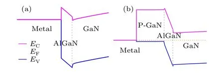
Due to the stronger depletion effect of PN junction, the channel electron concentration is lower at the same gate voltage, so the current density of the conventional HEMTs without the p-GaN layer is higher than that of the p-GaN HEMTs.Similarly, due to the existence of both Schottky contact and PN junction,the current density of the PSHG HEMTs is larger than p-GaN HEMTs, and the larger the proportion of p-GaN layer is,the lower the current density is.[14]In addition,due to the existence of Schottky gate,the distance between gate and channel is reduced, which can effectively modulate channel electrons. Therefore, with effective adjustment of the Schottky gate area,the gate control ability is improved,and the peak transconductance increases.[15]
In order to explore the mechanism of the threshold voltage characteristics, the channel electron concentration distribution of the p-GaN HEMTs,the 20%PSHG HEMTs and the conventional HEMTs under zero bias condition were plotted,as shown in the Fig. 6. It can be seen that due to the existence of p-GaN layer, the channel electron concentration below the p-GaN layer is almost depleted,which indicate that the threshold voltage of the PSHG HEMTs seems to have nothing to do with the p-GaN ratio. However, when the p-GaN ratio has been continuously reduced, and the PSHG HEMTs with 16%,12%,8%,4%and 2%of p-GaN ratio are simulated,respectively. The transfer characteristics curves are shown in Fig.7(a),and the variation curve of threshold voltage with different p-GaN ratio is shown in Fig.7(b).
It can be seen from the figure that when the p-GaN ratio is lower than 20%,the threshold voltage of the PSHG HEMTs can be negatively shifted, indicating that the depletion effect of the p-GaN layer begins to weaken. Meanwhile, when the p-GaN ratio reaches about 2%,the threshold voltage of PSHG HEMTs is exactly 0,which means that when the p-GaN ratio is less than 2%, p-GaN layer can no longer deplete the channel electrons,and the PSHG HEMTs will become a depletion device.
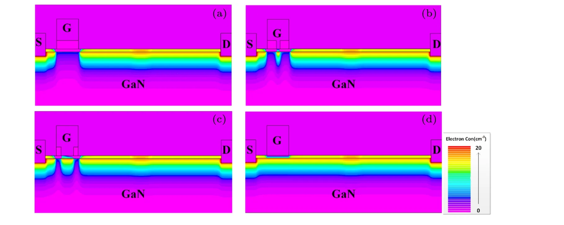
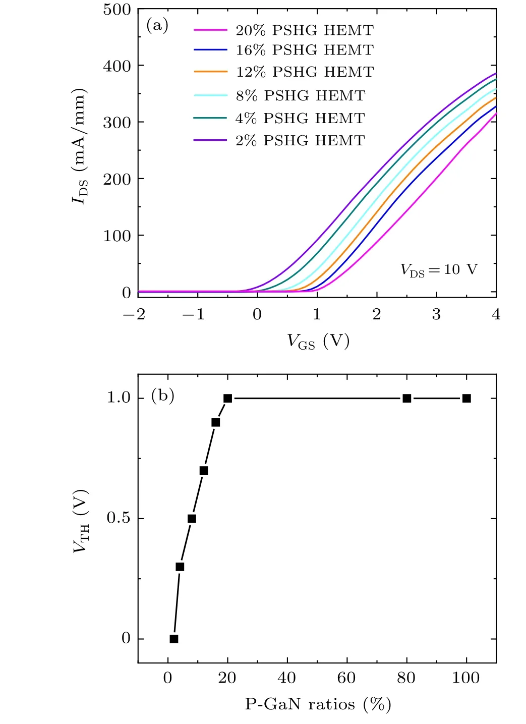
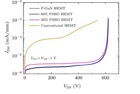
Figure 8 shows the comparison of the breakdown characteristics of the p-GaN HEMTs, 80% PSHG HEMTs, 20%PSHG HEMTs and the conventional HEMTs. The breakdown voltage of the devices is defined as the drain voltage when drain current is up to 1 μA/mm atVGS=VTH-1 V.The breakdown voltage of the conventional HEMTs is 540 V,while those of the p-GaN HEMTs and the PSHG HEMTs are 620 V.It is obvious that the pGaN layer can improve the breakdown voltage of AlGaN/GaN HEMT,but the reduction of p-GaN layer ratio has little effect on the reverse blocking capability of the device.
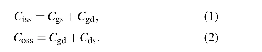
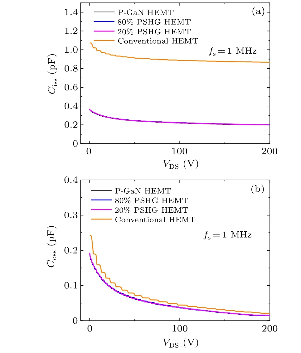
The switching characteristics of the devices are simulated to make a further comparison. The capacitance–voltage (C–V) curves of these four devices are showed in Fig. 9. The three inter-electrode capacitancesCgs,Cgd,andCdswere simulated,respectively,and then converted into the input capacitanceCissand the output capacitanceCossby using the following equations:[16]
Here,VDSwas set from 0 V to 200 V and allC–Vsimulations were conducted underVGS=0 V and simulation frequencyfs=1 MHz.[17]As shown in Fig.9,the gate capacitance of p-GaN HEMTs is lower than that of conventional HEMTs, because the p-GaN HEMTs is a series connection of Schottky barrier capacitance and PN junction capacitance. In addition,it is found that the gate capacitance of p-GaN HEMTs is very close to PSHG HEMTs,indicating that the p-GaN layer ratio can not strongly influence the switching characteristics.
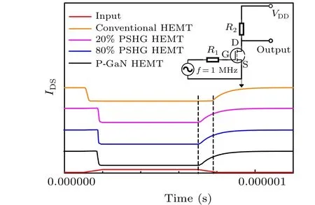
In order to show the switching speed of the device more intuitively, mix-mode simulation is used to compare the switching characteristics of the four devices, as shown in Fig.10.R1,R2andVDDare set to be 100 Ω,1000 Ω and 10 V in the circuit, respectively. It is obvious that the switching speed of devices with p-GaN layer is faster than that of conventional HEMTs. The p-GaN HEMTs and PSHG HEMTs almost have the same switching speed. These results are consistent with the simulation results ofC–Vcharacteristics.
4. Conclusion and perspectives
As a conclusion, a novel normally-off PSHG HEMT based on p-GaN HEMTs was proposed. Furthermore, the transfer characteristics, output characteristics, breakdown characteristics and switching characteristics of the devices were analyzed in detail by using Slivaco TCAD simulation software. The results show that with the decrease of p-GaN layer ratio, the on-state current density and transconductance of PSHG HEMTs increased,while the on-resistance decreased. The PSHG HEMTs with 20% p-GaN layer ratio show the best characteristics with the current density of 315 mA/mm and the peak transconductance of 122 mS/mm,respectively,which were 45%and 18%larger than that of the p-GaN HEMTs, respectively. In addition, the on resistance of PSHG HEMTs with 20% p-GaN layer ratio was reduced by 1.5 mΩ·mm compared with p-GaN HEMTs,showing better forward characteristics. The threshold voltage and breakdown voltage of PSHG HEMTs with different p-GaN ratios were 1.0 V and 620 V,respectively,which are close to p-GaN HEMTs. In addition, PSHG HEMTs have higher switching speed than conventional normally-on HEMTs,and the p-GaN layer ratio had little effect on the switching speed of PSHG HEMTs.
Acknowledgments
This work was supported by the National Natural Science Foundation of China (Grant No. 62004150), Postdoctoral Science Foundation of China(Grant No.2018M643575),the Fundamental Research Funds for the Central Universities, and the Innovation Fund of Xidian University (Grant No.JB211104).
- Chinese Physics B的其它文章
- Switchable terahertz polarization converter based on VO2 metamaterial
- Data-driven parity-time-symmetric vector rogue wave solutions of multi-component nonlinear Schr¨odinger equation
- Neutron activation cross section data library
- Multi-phase field simulation of competitive grain growth for directional solidification
- A novel similarity measure for mining missing links in long-path networks
- Effects of electrical stress on the characteristics and defect behaviors in GaN-based near-ultraviolet light emitting diodes