Enhanced photoluminescence of monolayer MoS2 on stepped gold structure
2022-08-31 09:59:28YuChunLiu劉玉春XinTan譚欣TianCiShen沈天賜andFuXingGu谷付星
Chinese Physics B 2022年8期
Yu-Chun Liu(劉玉春), Xin Tan(譚欣), Tian-Ci Shen(沈天賜), and Fu-Xing Gu(谷付星)
School of Optical-Electrical and Computer Engineering,University of Shanghai for Science and Technology,Shanghai 200093,China
Keywords: MoS2,stepped gold,heterostructures,enhanced photoluminescence
1. Introduction
Molybdenum disulfide (MoS2), as a typical twodimensional (2D) transition metal dichalcogenides (TMDC),has drawn much attention due to its outstanding properties and various promising applications.[1–4]Numerous efforts have been made to tune excitonic photoluminescence(PL) and optoelectrical property of monolayer MoS2, showing its great potentials in nanophotonics, micro-lasers, optoelectronic devices,etc.[5–8]These promising investigations indicate that the MoS2/Au heterostructure plays an important role due to the surface plasmon resonance and charge transfer effects across the interface. Various Au nanostructures have been utilized to modulate the PL and optoelectrical performance of 2D MoS2through surface plasmon effect, including nanoparticles,nanorods,nanotriangles,nanoholes and nanostripe arrays.[9–14]The surface plasmons generated in the metallic nanostructures are conducive to generating excitons and achieving higher optical absorption via enhancing localfield coupling in MoS2/Au heterostructures, leading to dramatic enhancement of PL and Raman emission.[15,16]Monolayer MoS2on Au grating array was used to explore the strong coupling regime of ultrafast plasmonic hot electron transfer,localized surface plasmons (LSPs) and surface plasmon polaritons(SPPs),where SPPs with a unique nonradiative feature can reuse the radiative energy of LSP and contribute to hot carrier generation.[17]Such prior researches suggest that the different MoS2/Au heterostructures can create new phenomena and play an important role in tuning the PL and optoelectrical properties of monolayer MoS2. However, these reported studies of MoS2/Au heterostructures have mainly focused on different Au nanostructures.
Except for the surface plasmon effect due to Au nanostructures, the PL tailoring of monolayer MoS2by Au continuous thin films is still limited. The MoS2/Au heterostructures can suppress the charge recombination by efficient charge transfer, which was critical for efficient exciton dissociation and good electron transport. The PL quenching of monolayer MoS2on flat Au surface by exfoliation method and by the chemical vapor deposition (CVD) method have been reported.[18,19]The PL quenching phenomenon observed in a MoS2/Au junction was due to highly efficient interlayer charge transfer as compared with that in MoS2/SiO2.[20]The temperature increase and annealing processing reduced the interlayer spacings between the monolayer MoS2and metals,which can promote the interlayer charge transfer. It was also reported the vacuum annealing can induce the oxygen atoms to be removed from sulfur vacancies and reduce the inherent van der Waals gap at the MoS2/Au interface, which facilitates the trapping of photo-generated electrons and the carrier separation.[21]Micro-Raman spectra revealed that the variation of out-ofplane A1gmode strongly is correlated with the strength of the MoS2–Au interaction,which can be affected by the roughness and cleanliness of the underlying Au.[22]The Au substrates with TiO2spacer layers of different thickness values were reported to be able to enhance the PL emission of monolayer MoS2on Au due to the Fabry–Perot interference.[23,24]The PL intensity of MoS2/TiO2/Au with a 41-nm-thick TiO2layer was observed to increase by 15 times,which is attributed to the fact that the local field enhancement originating from the metal surface roughness became dominant for thin spacer less than~10 nm. However,the evolution of excitonic PL change and electron transfer of the MoS2/Au heterostructures have been still unclear so far. In the present work, we investigate the excitonic PL emission of continuous CVD-grown monolayer MoS2on Au thin film with a stepped structure. The enhanced PL emissions observed in the MoS2/Au heterostructures in our experiments are different from the reported quenched or reduced PL emission from monolayer MoS2on the flat Au thin film. The A-excitonic PL emissions in MoS2/Au-60 heterostructures exhibit 2.4-fold and 3.3-fold PL intensities at the peak energy, in comparison with those in MoS2/Au-100 and MoS2/SiO2. The PL enhancement in MoS2/Au heterostructure can be attributed to the different charge transfer effects.
2. Experimental method
The stepped Au structures with the thickness values of~60-nm and~100-nm Au were built by sputtering on an Si/SiO2substrate. MoS2monolayers were grown on SiO2/Si substrates by the traditional CVD method in a furnace by using sulfur powder and molybdenum (VI) oxide powder as precursors.[25]Then the continuous MoS2monolayer was transferred to a target stepped Au structures on SiO2/Si substrate by using poly(methyl methacrylate)(PMMA)and polydimethylsiloxanes (PDMS). After being transferred, the remaining MoS2on the target substrate was rinsed by acetone to remove organic residues. The 2D MoS2/Au heterostructures were successfully built by transferring the MoS2monolayers onto the Au stepped structures with different thicknesses, respectively. The micro-PL and micro-Raman spectra were measured by a microscope system(Renishaw inVia)at room-temperature. The samples were excited by using a 532-nm (2.33 eV) continuous wavelength (CW) laser that is focused by a microscope objective lens(×50)into an about 2-μm-diameter spot. The excitation power was kept less than 0.2 mW to minimize the laser heating effect. The surface morphology and surface potential of MoS2and Au films were measured using the atomic force microscopy (AFM, Bruker)under the atmospheric environment.
3. Results and discussion
The PL measurements of MoS2/Au heterostructures consisting of monolayer CVD-grown MoS2and Au thin film were performed at room temperature under ambient atmosphere by using 532-nm CW-laser excitation. As shown in Fig. 1, the MoS2/Au heterostructures exhibit enhanced PL emission with blue-shifted PL peak in comparison with MoS2/SiO2. The A-excitonic PL peaks are located at 1.871 eV, 1.891 eV, and 1.894 eV, respectively for MoS2monolayers transferred on SiO2, Au (60 nm), and Au (100 nm). The PL peak of MoS2around 2.03 eV nm is attributed to the radiative recombination of B excitons. The excitonic PL emissions in MoS2/Au-60 heterostructures exhibit 2.4-fold and 3.3-fold PL intensities in comparison with those of MoS2/Au-100 and MoS2/SiO2.
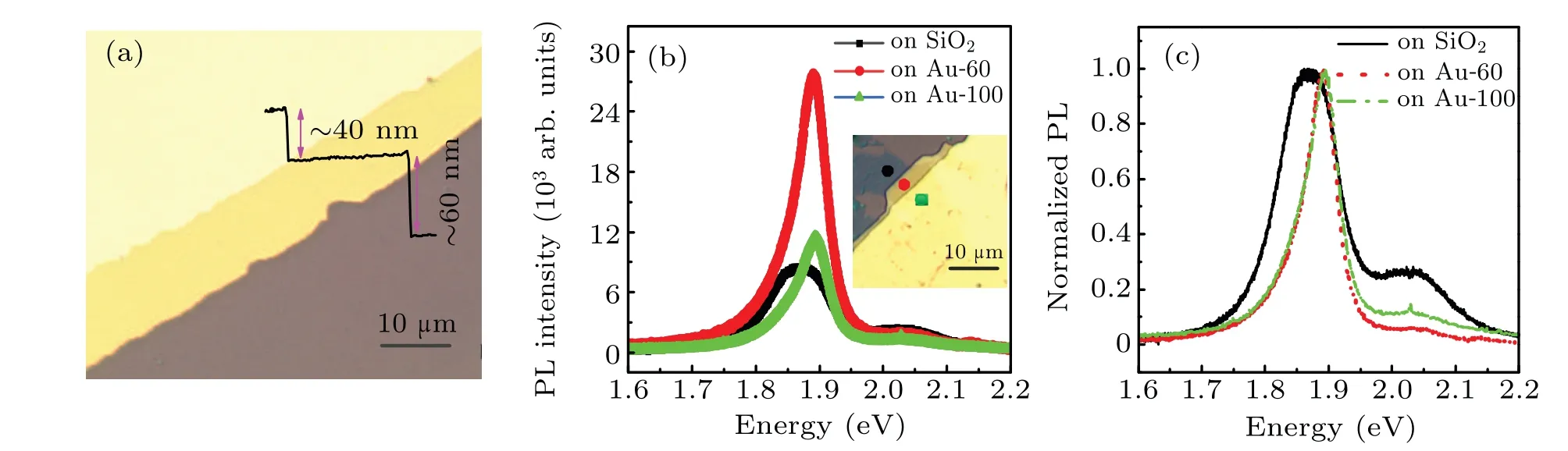
Fig.1. (a)Optical image of Si/SiO2 substrate and stepped Au structure with ~60-nm and ~100-nm-thick Au layer;(b)PL spectra and(c)normalized PL intensity for transferred continuous CVD-grown monolayer MoS2 on Si/SiO2, Au-60, and Au-100. Black, red, and green lines refer to the PL emissions of MoS2 at the position of the black,red,and green dots in panel(b),respectively.
The PL spectra are fitted by Lorentzian curves with three peaks denoted by the emission of neutral excitons(A0),trions(A?), and B excitons at 1.895 eV, 1.855 eV, and 2.03 eV, respectively,as shown in Figs.2(a)–2(c). Compared with MoS2on SiO2, the MoS2/Au (60 nm) heterostructure shows significant A-excitonic PL enhancement, and suppressed B excitonic PL, while the A-excitonic PL of MoS2/Au (100 nm)decreases slightly. As shown in Figs.2(d)–2(e),the excitonic PL intensity from A0(IA0) are obviously stronger than those form A?(IA?) in MoS2/Au heterostructures. The estimated PL intensity ratio A?/A0decreases from 4.03 in MoS2/SiO2to 0.80 in MoS2/Au-60, and 0.62 in MoS2/Au-100. The A?recombination emission takes less spectral weight after the MoS2has been transferred onto the Au thin film than onto the SiO2/Si, indicating the decrease of electron density in monolayer MoS2/Au. The electron densitynelin monolayer MoS2can be estimated from the trion PL spectral weightIA?/Itotalanalysis according to mass action model based on the dynamic equilibrium among A0,A?,and free electrons as given below:[26]
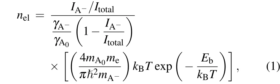
wherekBis the Boltzmann constant,Ebis the trion binding energy(~20 meV),m0is the mass of free electron,me(0.35m0),mA0(0.8m0),andmA?(1.15m0)are the effective mass of electron, A0, and A?, respectively,γA?/γA0refers to the relative decay rate,and the value is~0.15.[27]
As shown in Fig.2(f),the corresponding estimated electron densities are 2.0×1013cm?2and 1.55×1013cm?2in MoS2/Au-60 and MoS2/Au-100 respectively, both of which are much smaller than that in MoS2/SiO2(1.01×1014cm?2).The PL emissions from MoS2on Au are obviously higher than on SiO2, which is also in agreement with a dominant PL contribution from A0emission in MoS2/Au heterostructure with enhanced transition from A?to A0. Furthermore,the B-excitonic PL emissions almost vanish in MoS2/Au-60 and MoS2/Au-100.
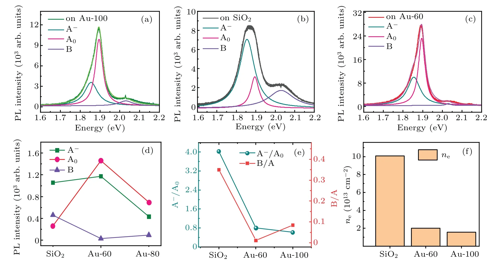
Fig. 2. (a)–(c) Representative PL spectra fitted by Lorenz function with three PL peaks (A0, A?, and B) for MoS2 on SiO2, Au-60, and Au-100; (d) PL intensity from A0,A?,and B,(e)PL spectral weights and(f)estimated electron density in MoS2 on SiO2,Au-60,and Au-100.
Fig.3. (a)Raman spectra,(b)E12g peaks,and(c)A1g peaks for transferred MoS2 on SiO2,Au-60,and Au-100.
Generally,the enhanced PL intensity in MoS2can be ascribed to the chemical doping effect, the plasmon effect, the train effect, and charge transfer effect. There is no additional chemical doping in our experiment. Since the roughness of Au film is small (< 1 nm), the localized plasmon effect of MoS2on Au film is negligible in comparison with the effect of Au nanoparticles and Au plasmonic nanostructures. To uncover the enhanced PL emission in MoS2/Au heterostructure, the transferred monolayer MoS2on SiO2and stepped Au are further characterized by Raman spectroscopy. Figure 3 shows that the Raman peaks of MoS2on SiO2are at 384.58 cm?1, which is caused by the in-plane vibration of S–Mo–S atom (E12gmode), and 404.71 cm?1, which is induced by the out-of-plane vibration of S atoms (A1gmode).The frequency difference in frequency between the Raman peaks of the transferred monolayer MoS2on the SiO2/Si structure is 20.13 cm?1, in accordance with the reported value of transferred monolayer MoS2. The E12gand A1gpeaks of Raman spectra are 384.15 cm?1and 405.09 cm?1for MoS2/Au(60 nm), and 384.26 cm?1and 405.63 cm?1for MoS2/Au(100 nm). The obvious red shift of E12gpeak and the blue shift of the A1gpeak for MoS2/Au with respect to MoS2on SiO2are observed. The A1gpeak is obviously shifted by~0.92 cm?1,indicating interaction between MoS2and Au. The difference in frequency between E12gand A1gpeak positions of MoS2on Au-60 and Au-100 are ?ωAu?60=20.94 cm?1and?ωAu?100=21.37 cm?1,respectively.
Generally,E12gand A1gpeak shifts are associated with the strain and doping effect in MoS2. Raman peak shifts vary linearly with biaxial strain (from 0 to 1%), and the slopes are?4.48 cm?1and?1.02 cm?1per 1%of biaxial strain for E12gand A1gmodes, respectively, while the A exciton peak exhibits a linear red-shift rate of?0.11 eV per 1% of biaxial tensile strain.[28]Furthermore, the electron doping density of 1.8×1013cm?2could lead to?4-cm?1shift in the A1gmode and?0.6-cm?1shift in the E12gmode.[29]It has been reported that A1gmode exhibits peak shift mostly dependent on the charge doping,while E12gmode was more sensitive to the tensile strain resulting from MoS2.[30–32]Comparing with the reference case of a freestanding 1-L MoS2with E12gand A1gpeak frequencies at 385 cm?1and 405 cm?1, the biaxial tensile strain and n-type doping(electron-doping)for MoS2on SiO2are estimated at~0.087%and 0.91×1012cm?2,respectively.A strain and a p-type doping density in MoS2/Au-60 are estimated at~0.200%and~1.32×1012cm?2,while the tensile strain and p-type doping (hole-doping) in MoS2/Au-100 are estimated at~0.193%and~3.72×1012cm?2,respectively.The negligible difference in tensile strain suggests that there is no obvious difference in strain effect between MoS2/Au-60 heterostructure and MoS2/Au-100 heterostructure. The estimated p-type doping in MoS2/Au can be attributed to the electron transferring from MoS2to Au,which is in agreement with excitonic PL emission result. Since the A-excitonic PL can exhibit a linear peak red-shifting and rapid intensity decreasing with biaxial tensile strain increasing,[33,34]the greater enhancement of PL intensity in MoS2/Au-60 is due to the difference in electron transfer effect rather than the small strain effect difference between MoS2/Au-60 and MoS2/Au-100. Furthermore, the Raman intensity per area from the suspended region was reported to be 50%–100% higher than that from the supported region in the literature.[35]The higher intensity in MoS2/Au-60 than in MoS2/Au-100 can be attributed to the less contact between MoS2layer and Au-60, which is in accord with the above estimated p-type doping density.
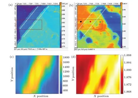
Fig.4. (a)and(b)Morphology and SKPM surface potential,(c)PL intensity mapping,(d)PL emission peak mapping for monolayer MoS2 transferred on Si/SiO2 and stepped Au structure.
To further study the charge transfer between MoS2and underlying substrate, scanning Kelvin probe microscopy(SKPM)measurement with an ElectriMulti75-G probe is carried out so as to obtain the morphology and surface potential information of samples simultaneously. The surface potential of monolayer MoS2and Au can be measured by the contact potential difference, which refers to the difference in work function between tip (φtip) and sample (φtip), thuseVsurf=(φtip?φsample). The morphology and surface potential of MoS2/SiO2and MoS2/Au heterostructures are shown in Figs. 4(a) and 4(b). The difference in measured contact potential of MoS2/SiO2(black dot), MoS2/Au-60 (red dot), and MoS2/Au-100 (green dot) are 0.490 V, 0.470 V,and 0.480 V, respectively, while the contact potential difference of Au is 0.383 V. In contrast with the work function of Au (~5.1 eV), surface work function of MoS2/SiO2,MoS2/Au-60, and MoS2/Au-100 without laser illumination are 4.993 eV, 5.013 eV, and 5.003 eV, respectively. According to the 2D model of electron gas at non-zero temperature,the Fermi energy shift in MoS2monolayer(?EF=πˉh2?n/me)can be calculated from the electron density change by using an electron band mass ofme=0.35m0, wherem0is the electron mass. Comparing with MoS2on SiO2, the surface potential of MoS2/Au-60 and MoS2/Au-100 are reduced by 20 mV and 10 mV, respectively, indicating that the calculated electron density differences are 2.92×1012cm?2and 1.46×1012cm?2, respectively. The calculated electron density differences from surface potential without laser illumination are much smaller than that estimated from A?/A0ratio,suggesting that the electron density of MoS2is increased under laser illumination.
Figures 4(c) and 4(d) refer to the PL intensity mapping and PL peak mapping of MoS2in the region of black rectangle in Fig.4(a). The difference in PL intensity in MoS2/SiO2,MoS2/Au-100, and MoS2/Au-60 can be attributed to the different charge transfer situations. As Kwonet al.reported,the measured surface potential of monolayer MoS2in contact with the Au stripe in dark is greater than that of the suspended MoS2surface,while the surface potential of MoS2on Au stripe is smaller than that of the suspended MoS2surface under light illumination with a wavelength of 532 nm.[36]Furthermore,Liet al.reported that the work function is 4.93 eV for CVD-grown monolayer MoS2on an Si/SiO2substrate and 5.50 eV for that on a Pt substrate in dark,which decreases to 4.74 eV and increases to 5.56 eV under 355-nm laser excitation, respectively.[37]Therefore, we consider that the work function of MoS2/SiO2will decrease, and the work function of MoS2/Au-60 will be higher than that of MoS2/Au-100 under 532-nm laser excitation. Thus, the excess electrons in MoS2/Au-100 can move towards the MoS2/Au-60 under laser illumination as shown in Fig.5(a). Additionally,the electrons in MoS2/Au-100 can also be readily transferred into the Au film at the MoS2/Au interface. Thus, as shown in Fig. 5(b),the electrons transfer in MoS2occurs between MoS2/SiO2,MoS2/Au and the underlying Au film,which will finally lead to a transient dynamic equilibrium and band alignment under the laser excitation.[38]As a result,the decreasing of electron density in MoS2/Au gives rise to the blue-shift of PL peak and PL enhancement of A0radiative recombination. It should be noted that the laser used in our study has a size of~2μm in diameter and average power of less than 0.2 mW.During the PL measurement, MoS2/SiO2, MoS2/Au-100, and MoS2/Au-60 cannot be irradiated simultaneously. The photo-induced electrons from irradiated MoS2region can drift to um-irradiated region. The dynamic equilibrium will be different when the laser irradiates the MoS2/SiO2,MoS2/Au-100,and MoS2/Au-60, respectively. In addition, since O2/H2O molecules from ambient air can be physically and chemically adsorbed by the defects on MoS2surface, the charge transfer can also occur between monolayer MoS2and gas molecules. The PL emission of MoS2/Au heterostructures can be tuned by changing the charge transfer between MoS2and gas molecules, which will be further investigated in the future.
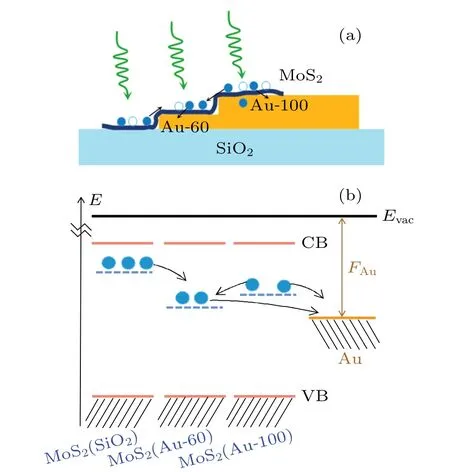
Fig.5.Schematic illustrations of(a)charge transfer and(b)expected electron transfer at Fermi energy levels between MoS2/SiO2,MoS2/Au,and underlying Au under laser excitation.
4. Conclusions and perspectives
In this work,we have built MoS2/Au heterostructures by transferring CVD-grown monolayer MoS2onto a stepped Au structure with Au thickness of~60 nm and~100 nm on Si/SiO2substrate. The MoS2/Au-60 and MoS2/Au-100 heterostructures exhibit enhanced PL emission with blue-shifted PL peaks in comparison with MoS2/SiO2. Furthermore, the PL intensity of the MoS2/Au-60 sample is twice larger than that of the MoS2/Au-100 sample. The difference in enhancement extent of excitonic PL among the MoS2/Au heterostructures can be attributed to the difference in their charge transfer effects modified by the stepped Au structure,which determines the PL emission from A0and A?. Our results demonstrate a novel method to quantitatively tune the excitonic PL emission from MoS2/Au vertical heterostructure,and are also conducive to the understanding of the charge transfer between CVD-grown MoS2and Au,and provide a valuable insight into the excitonic PL and optoelectrical properties of MoS2/metal heterostructures.
Acknowledgements
We thank Dr. Zhaoqi Gu and Prof. Jiaxin Yu for helpful suggestions.
Project supported by the China Postdoctoral Science Foundation(Grant No.2020M671168)and the National Natural Science Foundation of China(Grant No.62075131).
- Chinese Physics B的其它文章
- Magnetic properties of oxides and silicon single crystals
- Non-universal Fermi polaron in quasi two-dimensional quantum gases
- Purification in entanglement distribution with deep quantum neural network
- New insight into the mechanism of DNA polymerase I revealed by single-molecule FRET studies of Klenow fragment
- A 4×4 metal-semiconductor-metal rectangular deep-ultraviolet detector array of Ga2O3 photoconductor with high photo response
- Wake-up effect in Hf0.4Zr0.6O2 ferroelectric thin-film capacitors under a cycling electric field