Monolayer MoS2 of high mobility grown on SiO2 substrate by two-step chemical vapor deposition
2022-08-31 09:55:46JiaJunMa馬佳俊KangWu吳康ZhenYuWang王振宇RuiSongMa馬瑞松LiHongBao鮑麗宏QingDai戴慶JinDongRen任金東andHongJunGao高鴻鈞
Chinese Physics B 2022年8期
Jia-Jun Ma(馬佳俊) Kang Wu(吳康) Zhen-Yu Wang(王振宇) Rui-Song Ma(馬瑞松)Li-Hong Bao(鮑麗宏) Qing Dai(戴慶) Jin-Dong Ren(任金東) and Hong-Jun Gao(高鴻鈞)
1Institute of Physics,Chinese Academy of Sciences,Beijing 100190,China
2School of Physical Sciences,University of Chinese Academy of Sciences,Chinese Academy of Sciences,Beijing 100190,China
3CAS Key Laboratory of Nanophotonic Materials and Devices,CAS Key Laboratory of Standardization and Measurement for Nano-technology,National Center for Nanoscience and Technology,Beijing 100190,China
4CAS Center for Excellence in Topological Quantum Computation,University of Chinese Academy of Sciences,Beijing 100190,China
Keywords: chemical vapor deposition(CVD),scanning tunneling microscope(STM),MoS2,transport
1. Introduction
The 2H-phase molybdenum disulfide(MoS2)monolayer,a two-dimensional semiconductor with relatively large direct band gap of 1.8 eV and lack of dangling bonds, has attracted much attention in the fields of flexible electronics,[1]optical devices,[2]field effect transistors (FET),[3]and non-volatile memory devices.[4]Similar to other 2D materials, the monolayer MoS2can be obtained by mechanical exfoliation as well as CVD method.Although the exfoliated flakes[5]have shown excellent electrical properties,the drawbacks of small size and low production hinder their further development. Indeed, the CVD method can directly grow monolayer MoS2with high domain size and production, where the molten glass[6]or the sapphire[7,8]was used as target substrate. However,the subsequent transfer to the SiO2or high-ksubstrates for the following device fabrication is much likely to degrade MoS2’s quality.Although small size of MoS2has been directly synthesized on SiO2,[9,10]the new CVD method to grow larger size MoS2is needed.
To figure out the relationship between the transport properties and the atomic structures of MoS2,we can use scanning tunneling microscope (STM) to access its electrical performance and lattice structure simultaneously.[11]However, the reports about direct STM characterization of MoS2on the insulating substrate rather than metal or graphite substrates are rare due to poor sample cleanliness and difficulty in making ohmic contact with the TMDs films.[11–13]Nevertheless, the sample surface might be destroyed during the fabrication of the bias electrodes in these reports.[14,15]In fact, the fourprobe STM (4P-STM) with the movable probes is ideal by utilizing the grounding probe to touch the sample directly and the STM probe to scan across the sample.[16]The optical microscope could also help to identify the relative position between the probes and the small samples.[17]Without microfabrication process, sample destruction is avoided during the STM characterization. And the intrinsic physical properties could be conserved and revealed.
In this study,we design a two-step ambient pressure CVD(APCVD)procedure to synthesize large-size monolayer MoS2on the SiO2substrate. Various characterization techniques are adopted to prove the high quality of the as-grown material.The direct 4P-STM characterization reveals the surface electronic information,which is also verified in the following twoterminal transport measurements. Furthermore, the relatively high carrier mobility extracted from the van der Pauw measurements confirms the high quality of the CVD-grown materials again.
2. Experiments
Our two-step APCVD[18]procedure to grow large domain 2H-MoS2on SiO2/Si substrate is shown in Fig. 1(a).In most previous works,[7,19–25]the MoO3powder is utilized as the Mo source and the APCVD is involved. The MoO3powder is reduced by the sulfur to form suboxide MoO3?xand the suboxide diffuses to the substrate and further reacts into MoS2.[19]But the MoS2synthesized at the surface of the MoO3powder during the CVD process could hinder its subsequent evaporation.[26]The consumption of MoO3powder is relatively high in previous articles,[20,27–29]which is in the range of 1 mg to 100 mg. In contrary, we chose the MoO3single crystal flakes synthesized on the mica substrate in the first CVD step as the Mo precursor of the second CVD step.The weight of MoO3flakes on our mica substrate is estimated to be smaller than 25 μg. The utilization of the MoO3flakes could reduce the MoO3consumption because of its large specific surface area, which is beneficial to its effective evaporation. Therefore,this two-step growth method can be extended to grow inch-scale MoS2thin film by enlarging the area of MoO3on the mica substrate.
3. Results and discussion
In the first step, one-zone tube furnace is utilized, where the MoO3single crystal is directly grown on the mica substrate by oxidizing the Mo foil in the air condition at 540?C for 40 min.[30,31]A piece of Mo foil is placed in a quartz boat and the freshly exfoliated mica surface is placed upside down on the same quartz boat, as shown in the upper section of Fig. 1(a). The optical image of the synthesized MoO3crystal on the mica substrate is shown in Fig. 1(b) and its high quality is confirmed in Fig.S1.
In the second step, the two-zone APCVD is adopted to synthesize the monolayer MoS2,as displayed in the lower section of Fig.1(a). The pre-synthesized MoO3on the mica substrates is in the growth quartz boat where the clean SiO2/Si target substrates are placed face-down with a distance about 2 mm. The sulfur source(Alfa Aesar, 99.9%, 400 mg)in the other quartz boat is placed upstream to the growth boat with Ar as the carrying gas in a two-zone tube furnace. The source and growth temperatures are 140?C and 850?C,respectively.
Figures 1(c)–1(e) are the large-scale optical images of the monolayer MoS2synthesized at different growth temperatures. The corresponding temperature is listed at the left top section of each image. We can clearly see that 850?C is the most suitable growth temperature regarding the nucleation centers and the domain size. Noting that the large size MoS2triangle domains are formed in a relatively high density.Some obvious nucleation centers with large optical contrast can be easily identified within some domains.[32]When the nucleation centers lie close to each other,the domains tend to merge into a larger one, thus leading to a polycrystalline nature. The uniform contrast indicates all these MoS2domains share the same thickness.
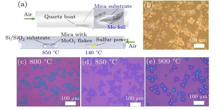
Fig.1. Synthesis of the CVD-grown monolayer MoS2. (a)Schematic illustration of the two-step CVD process. The MoO3 crystal is grown on the mica substrate during the first step. Then the monolayer MoS2 crystal is synthesized on the SiO2 substrate by using the first-step product,i.e.,MoO3 single crystal,as the Mo source. (b)Large-area optical image of the MoO3 on the mica substrate in the first-step CVD process. (c)–(e)Large-scale optical images of the MoS2 products at different growth temperatures of 800 ?C (c),850 ?C,(d)and 900 ?C(f),respectively.
In typical preparation process, the furnace is purged by pure Ar for 15 min to remove the air,followed by Ar carrying gas flowing in at a rate of 100 sccm(standard cubic centimeter per minute). Then the sulfur zone and the growth zone are heated to the target temperature simultaneously. The growth time is set as 15 min. After that, the furnace naturally cools down to the room temperature and large-sized MoS2will be synthesized on the SiO2/Si substrate.
We employed various characterization techniques to identify the topography and structure of the CVD-grown monolayer MoS2, including optical microscope (OM), atomic force microscope(AFM),Raman and photoluminescence(PL)spectra. Figure 2(a)exhibits a zoom-in optical image of a single crystal MoS2flake with the edge length up to 110 μm.Some monolayer islands are also present at the center of the beneath monolayer,which is commonly observed in the CVDsynthesized materials.[33]The triangle MoS2flake is a single crystal,whose edge termination is either molybdenum zigzag(Mo-zz)or sulfur zigzag(S-zz)that are the two most energetically stable edge orientations.[27]The AFM image in Fig.2(b)illustrates the topography features across the edge of the domain. Note that the surface of MoS2is flatter than that of bare SiO2substrate,with some micron-scale monolayer MoS2distributing randomly in the center.[33]The thickness of the upper MoS2is about 0.6 nm,which is identical to that of monolayer MoS2.[20]To further validate the structure of the MoS2, the Raman spectrum is collected at the monolayer region. The Raman E12gand A1gpeaks are located at 382.8 cm?1and 401.4 cm?1with the full width at half-maximum (FWHM)of 5.6 cm?1and 7.8 cm?1in Fig. 2(c), indicating the density of defects of this sample is relatively low.[34]The peak position distance between the two modes is 18.6 cm?1, illustrating the monolayer nature of our samples. Furthermore,the PL spectrum is also measured in Fig.2(d),exhibiting a dominant A-exciton peak around 1.81 eV with a full width at halfmaximum(FWHM)of 65 meV,which is comparable to other monolayer MoS2.Another lower peak at 1.94 eV should be attributed to the B exciton.[22,35]Therefore,we can declare that our monolayer MoS2is of high quality.
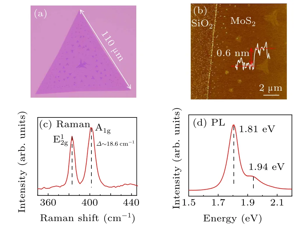
Fig.2. Characterization of CVD-grown monolayer MoS2. (a)Zoom-in optical image of a monolayer triangle MoS2flake with the edge length up to 110μm. Some MoS2 islands locate on the center of the beneath monolayer MoS2. (b)Atomic force microscope(AFM)image of one edge of monolayer MoS2. The surfaces of MoS2 and bare SiO2 substrate show totally different features. The thickness of the upper MoS2 is around 0.6 nm. (c)Representative Raman spectrum of the monolayer MoS2 on SiO2 shows two distinct vibration modes located at 382.8 cm?1 and 401.4 cm?1 with the full width at half-maximum(FWHM)of 5.6 cm?1 and 7.8 cm?1,indicating the density of the defects of the sample is relatively low. (d)Representative PL spectrum of the monolayer MoS2 on SiO2 shows relatively high peak at 1.81 eV.Another lower peak at 1.94 eV is attributed to B exciton.
Most of the above-mentioned characterization methods are indirect tools to confirm the high quality of our samples, while STM, as an atomic structure imaging implement,could provide direct electronic information. Hence, we employed four-probe STM[17,36]to directly identify the electronic structure of our MoS2at room temperature. The MoS2is introduced into the loadlock chamber and annealed at 200?C overnight to remove the adsorbates before the STM measurements.[12]
Figure 3(a) shows the optical image of the STM experiment setup,where the upper tip is the STM tip while the lower one is the ground tip. In other four-probe STM works,the first grounding probe’s contacting samples was achieved with the help of scanning electron microscope(SEM)[37]or the capacitance meter.[38]While in our case,SEM could destroy the surface of two-dimensional materials and the relatively small area of samples could not lead to noticeable capacitance change.Thus, we designed a special method utilizing the piezoelectric effect of the piezoelectric ceramic embedded in the STM probes. Based on our home-upgraded four probe STM,[39]we could link the inner and outer electrodes of the ceramic tube to a voltmeter and use the coarse motor to move the probe approaching the sample step by step.[17]Once the probe touches the sample, a noticeable DC voltage difference could be detected between the two electrodes immediately. Thanks to the small distance per step of the coarse motion,the probe’s contacting will not destroy the surface of sample and alter the intrinsic transport properties.
The large scale STM topography is exhibited in Fig.3(b).This typical STM image is collected near the monolayer islands based on the optical contrast and two regions can be easily clarified inferred from the different roughness distribution.In the monolayer region, the topography shows a root-meansquare (RMS) roughness of about 249 nm, which is comparable to the RMS roughness of the monolayer graphene on SiO2.[40]and the intrinsic RMS roughness of the substrate SiO2,[11]implying the synthesized MoS2is directly spread out onto the substrate and conforms well to the surface of SiO2,[11]which is relatively rough resulting from the dangling bonds.A series of nanometer-scale wrinkles could also be noticed over the whole area. The corrugated structure might act as carrier trapping center[41–44]which is also illustrated in the transport measurements. As for the bilayer region, the area appears higher and smoother, with the RMS roughness being 123 pm smaller than the monolayer area.[11]The smooth feature benefits from the increase in bending stiffness of the MoS2with thickness enlarging.[11]And this layer thicknessdependent roughness could be used to analyze the van der Waals interaction in this system.[11]
The zoom-in images of Fig. 3(b) in both monolayer and bilayer regions are listed in Figs.3(c)–3(e).The atomic resolution image of monolayer region marked by the yellow dashed square shows apparent hexagonal lattice as expected from the structure of the top sulfur atoms in Fig.3(c). The slight distortion of the hexagonal lattice should be attributed to the thermal drift of the STM probes. The obscure feature at the top section could be due to the residual insulating adsorbates[45]and the great roughness of the substrate. The inset of Fig. 3(c)is the corresponding fast Fourier transform (FFT) image exhibiting six bright spots in the six-fold symmetry. Some point defects are also present in the yellow solid square marked monolayer region shown in Fig. 3(d), which refer to the sulfur vacancies as the doping centers favoring the n-type transport behavior.[12]In contrary to the monolayer area,the atomic resolution image of the bilayer region marked by the green dashed square shows smoother feature in Fig. 3(e), in agreement with the result from the large scale STM topography. To measure the electronic spectrum of the monolayer MoS2, we conducted STS measurements. TheI–Vcurve and the corresponding dI/dVcurve are plotted in Fig.3(f). These spectra clearly demonstrate the presence of a tunneling gap displaying clear semiconductor features. The tunneling gap extends from?1.7 eV to +0.2 eV, forming the total gap of 1.9 eV,which is comparable to the band gap(1.8 eV)of the monolayer MoS2.[35]The Fermi level is near the edge of the conduction band,demonstrating the presence of the deep donor and leading to the n-type doping nature in accordance with other MoS2devices.[12]
To further evaluate the electrical properties of assynthesized MoS2, two-terminal field-effect transistors are fabricated. Figure 4(a) shows the optical image of the fabricated back-gate field effect transistor,where the triangle flake is scratched into the rectangle shape by a tungsten tip to avoid the electrical degradation during the etching process by reactive ion etching(RIE).The source and drain electrodes are defined by EBL and Cr(6 nm)/Au(60 nm)are deposited through the electron beam evaporation afterwards. Gate voltage is applied into the p++silicon to tune the carrier density. And all these measurements are conducted at room temperature in high vacuum(<10?5mbar).
Output characteristics of the device in linear scale as a function of back-gate voltages are displayed in Fig. 4(b) and the back-gate voltage ranges from?20 V to 80 V with the step of 10 V. The non-linear characteristics at lowVds(voltage between drain and source), also shown in supplementary Fig.S2(b),indicates the non-ideal ohmic contact between MoS2and metal electrodes.[46]For monolayer TMDs FETs,realizing the ideal ohmic contact is challenging owing to the destruction of atomic structure during the metal deposition process.[47]We can also note that velocity saturation can only occur at a relatively highVdsin our device when the gate voltage is big enough,implying our device is in the long-channel regime.[46]
The transfer characteristic, i.e., drain current (Ids) versus back-gate voltage (Vg), atVds=2 V in linear and semilogarithmic scales are plotted in Fig.4(c). Our device exhibits a distinct n-type behavior together with effective gate modulation. We also note that the device displays a low off-current of below 10?12A with the on/off current ratio of more than 107.The field effect electron mobility(μFE)can be extracted from the transfer curve based on the following formula:
whereCoxis the capacitance per area of 285 nm SiO2,?Ids/?Vgis the slope of the transfer curve across the entire linear region andL/Wis channel length/width(3.7μm/8.7μm).The as-calculatedμFEis about 13.7 cm2·V?1·s?1.
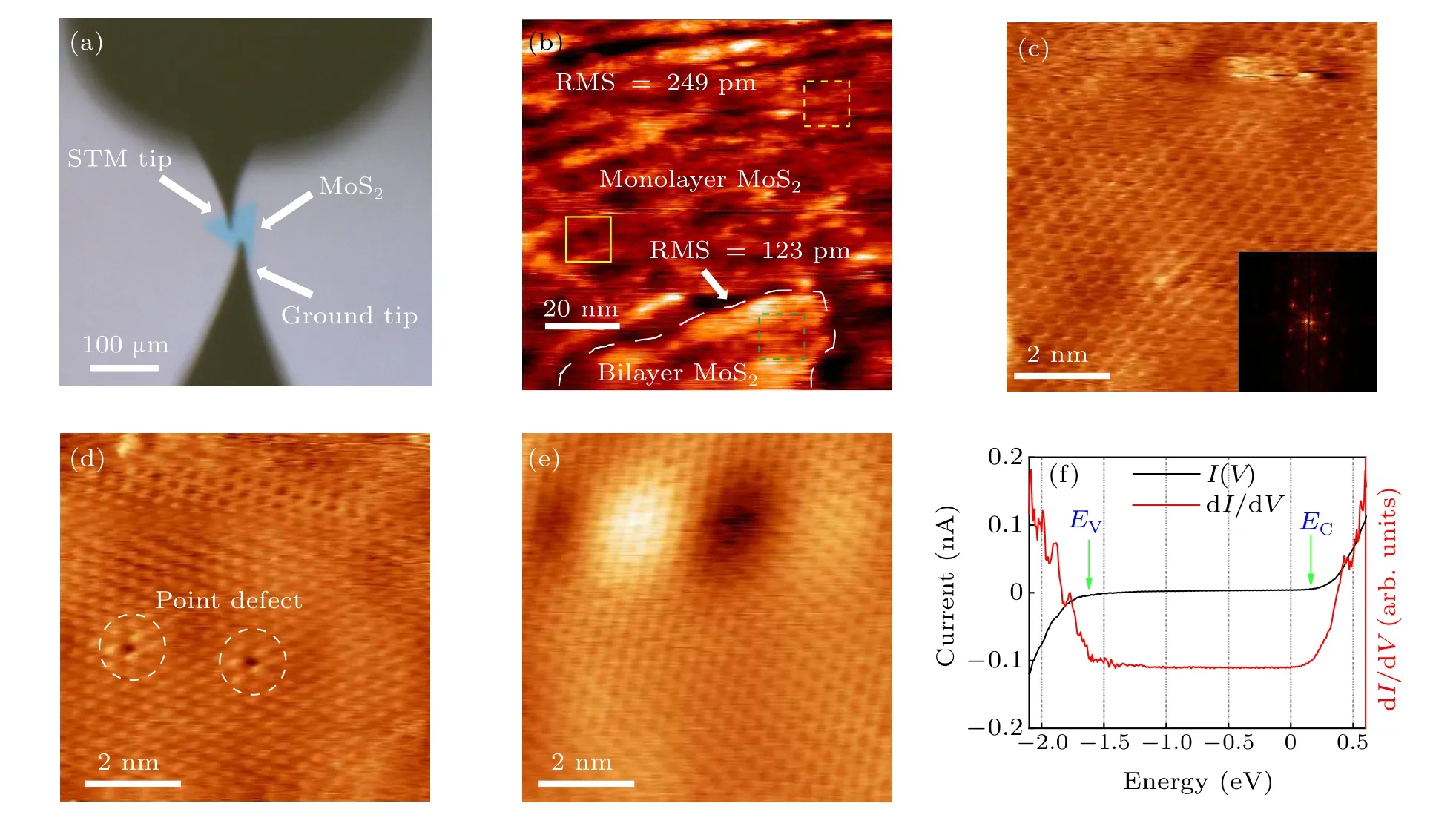
Fig. 3. The STM characterization of the CVD-grown monolayer MoS2. (a) Optical image of the STM setup. The upper tip is the STM tip and the lower one is the ground tip. (b) Large scale STM topography of the monolayer MoS2 near the monolayer island (Vbias =1 V, Isetpoint =100 pA). The area can be clarified into two regions based on the different roughness distribution. (c) Atomic resolution image of monolayer MoS2 shows hexagonal lattice(Vbias =2 V,Isetpoint =3.7 nA).The inset shows the FFT image of the atomic STM image. (d)Atomic resolution image of monolayer MoS2 near the point defects(Vbias=1 V,Isetpoint=3.7 nA),which refers to the sulfur vacancy favoring the n-type transport behaviors. (e)Atomic resolution image of the small bilayer region(Vbias=1 V,Isetpoint=1.0 nA).(f)The scanning tunneling spectrum(STS)of the monolayer MoS2,which shows the semiconductor features(Vbias=0.5 V,Isetpoint=500 pA,Vmod=40 mV).
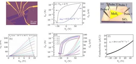
Fig.4. Two-terminal and direct four-probe transport measurements of the CVD-grown monolayer MoS2. (a)Optical image of the fabricated back-gate field effect transistor (FET). (b) Ids–Vds output characteristics with different back gate voltages. The non-linear characteristic at low Vds indicates the non-ideal ohmic contact between MoS2 and metal electrodes. The velocity saturation can only occur at a relatively high Vds when the gate voltage is big enough. (c)Transfer characteristic at Vds =2 V,exhibiting a distinct n-type behavior together with effective gate modulation. The mobility extracted from the curve is 13.7 cm2·V?1·s?1. (d)Corresponding Ids–Vg transfer characteristics at different bias voltages,showing obvious threshold voltage(VT)variations between forward and backward gate voltage sweeps. (e) The schematic diagram of the van der Pauw geometry with four probes placed at the three corners of the triangle and the periphery of one side of the triangle. (f)Conductivity of the monolayer MoS2 as a function of back-gate voltages calculated from van der Pauw geometry. According to the van der Pauw theory,the extracted electron mobility from the curve is 28.4 cm2·V?1·s?1.
TheVds-dependent transfer characteristics with back-gate voltage forward-backward sweeping are plotted in Fig. 4(d)both in linear and semi-logarithmic scales. Note that whenVgis 80 V, the drain currentIdsincreases linearly withVdsfrom 1 V to 5 V, which agrees with the output curve atVg= 80 V. And whenVdsincreases from 1 V to 5 V, the threshold voltage(VT)decreases from 25 V to 10 V,as shown in Fig. S2(a). What’s more, clear current hysteresis can be observed in the transfer curves, indicating that there areVTvariations between forward and backward sweeps resulting from variation of charge density in the gate voltage changing procedure.[33,48]These variations might be attributed to some electronic states at the interface between corrugated MoS2and SiO2surface,[41,42]the defect in the atomic structure or the adsorbates from air,[45,49]which may act as the charge trapping centers during the electrostatic doping process. They are all noticed in the above STM images.
As previously reported,in the traditional transport experiments, including the two-[50]and four-terminal[51]methods,the samples will go through the lithography process to fabricate the electrodes,where they will be contaminated unavoidably leading to electrical degradation effect. In contrary, the four-probe transport conducted by 4P-STM could avoid this drawback by using the long STM tips to contact the samples directly as electrodes,[36,42]thus preserving original shape of the samples and reflecting the intrinsic electrical properties.As for our 100μm domain size MoS2sample,it cannot be visualized as the infinite two-dimensional sheets regarding the comparable probe intervals (~40 μm) to the domain size,leading to the failure of the collinear and square configuration of the four-probe measurements.[37,38]Therefore,van der Pauw geometry,which can be applied to the thin films with arbitrary shapes,is employed to measure the transport properties of our CVD-grown MoS2.
In this case, the four probes, as the contact electrodes,are placed at the three corners of the triangle and the periphery of one side of the triangle, as shown in Fig. 4(e). The four probes are labeled as probe 1–4. The sheet conductivity as a function of back-gate voltages in a typical MoS2domain can be calculated based on van der Pauw method[52,53]and plotted in Fig. 4(f), exhibiting clear n-type transport behaviors in agreement with the two-terminal transport results.The electron mobility of 28.4 cm2·V?1·s?1can be calculated by linearly fitting the conductivity curve. The mobilities extracted from the direct four-probe measurements and twoterminal measurements are summarized in Table S1, and the electrical performances of other reported CVD-grown MoS2devices[7,19,27,54–58]are also included. We can notice the calculated mobility from the direct four-probe transport measurement is better than that of two-terminal measurement, indicating the direct four-probe method could reveal the intrinsic transport properties of our CVD-synthesized MoS2. The mobility of our MoS2is comparable to that of other reported CVD-grown MoS2confirming the high quality of our samples.
4. Conclusion
We design a two-step CVD method to synthesize large size single crystal MoS2monolayer. The OM, AFM, Raman and PL characterizations confirm its high quality and monolayer nature,while thein-situSTM characterization conducted by 4P-STM reveals the surface electronic information which is also verified in the two-terminal transport measurements.Simultaneously, direct four-probe transport measurement via van der Pauw geometry illustrates its relatively high carrier mobility among the CVD-grown MoS2. These synthesis and direct characterization methods could also be applied in the other 2D materials synthesized on the SiO2substrate.
Acknowledgments
Project supported by the National Natural Science Foundation of China (Grant No. 61888102), the National Natural Science Foundation of China (Grant No. 12004417), the National Key Research and Development Program of China (Grant Nos. 2018YFA0305800 and 2019YFA0308500), the National Natural Science Foundation of China (Grant No. U2032206), Chinese Academy of Sciences (Grant Nos. XDB36000000, YSBR-003, and 112111KYSB20160061), Strategic Priority Research Program of Chinese Academy of Sciences (CAS) (Grant Nos. XDB30000000 and XDB28000000), Youth Innovation Promotion Association of CAS (Grant No. Y201902), and CAS Project for Young Scientists in Basic Research (Grant No.YSBR-003).

- Chinese Physics B的其它文章
- Magnetic properties of oxides and silicon single crystals
- Non-universal Fermi polaron in quasi two-dimensional quantum gases
- Purification in entanglement distribution with deep quantum neural network
- New insight into the mechanism of DNA polymerase I revealed by single-molecule FRET studies of Klenow fragment
- A 4×4 metal-semiconductor-metal rectangular deep-ultraviolet detector array of Ga2O3 photoconductor with high photo response
- Wake-up effect in Hf0.4Zr0.6O2 ferroelectric thin-film capacitors under a cycling electric field