
Two-dimensional Sb cluster superlattice on Si substrate fabricated by a two-step method
2022-08-31 09:55:28RunxiaoZhang張潤瀟ZiLiu劉姿XinHu胡昕KunXie謝鹍XinyueLi李新月YuminXia夏玉敏andShengyongQin秦勝勇
Chinese Physics B 2022年8期
Runxiao Zhang(張潤瀟) Zi Liu(劉姿) Xin Hu(胡昕) Kun Xie(謝鹍)Xinyue Li(李新月) Yumin Xia(夏玉敏) and Shengyong Qin(秦勝勇)
1CAS Key Laboratory of Strongly Coupled Quantum Matter Physics,Department of Physics,University of Science and Technology of China,Hefei 230026,China
2International Center for Quantum Design of Functional Materials(ICQD),University of Science and Technology of China,Hefei 230026,China
Keywords: microstructure,nanoparticles,cluster superlattice,scanning tunneling microscope
1. Introduction
Nanoclusters have attracted lots of research interests due to their size-dependent structural, electronic and magnetic properties in recent years.[1–3]Compared to the bulk materials,unique surface-to-volume ratio and quantum confinement effect make nanoclusters promising catalysis and ideal platform to uncover new phenomena for nanoscience.[4–6]Cluster superlattice provides a promising candidate for studying the nanocluster, consequently establish an exciting field of research for nanoscience.[7–9]To grow the ordered cluster superlattice,self-assembly growth is an effective method in recent research,for instance,two-dimensional(2D)Co nanoparticles arranged in macroscopically phase-coherent superlattices are created by self-assembly on Au substrates.[10]Report also shows that ordered Al nanocluster arrays can be fabricated by self-assembly on Si(111).[11]Apart from the growth by self-assembly,a template growth with an ordered period substrate is also considered as an effective pathway to grow the cluster superlattice,in which the metal cluster can be deposited in the specific sites on the substrate. It was reported that graphene on Ir(111)can act as a promising substrate to grow Co, Ir and Pt cluster superlattices due to its periodic moir′e pattern.[12–14]Other substrates such as hexagonal boron nitride on Ir(111)or Rh(111)can also be a compatible template to grow metal nanocluster superlattices.[15,16]
So far, most of the cluster superlattices have been focusing on transition metals. Recently, antimony (Sb) as a semimetal element has attracted research interests due to the unique physical properties. Bulk antimony is a semimetal,however,a semiconductor–semimetal crossover occurs at one atomic layer thickness.[17]Moreover, monolayer antimony is predicted to harbor quantum spin Hall effect.[18–20]Consequently,finding an effective growth method for the Sb cluster superlattice is essential for providing the platform to explore the novel properties of antimony nanocluster. In addition, as the electronic and magnetic properties of the nanocluster are closely related to their structures, the study of the nanocluster’s atomic structure in the superlattice is also crucial.[21,22]However, the experimental research on the cluster superlattice, especially combined research of the growth method and their atomic structures are still lacking.
In this work, we have successfully fabricated twodimensional Sb cluster superlattice on Si substrate by a twostep method and characterized the atomic structures by scanning tunneling microscopy (STM), where the self-assembled Sb cluster superlattice shows a hexagonal array. Furthermore,high resolution STM measurements and scanning tunneling spectroscopy (STS) measurements have been carried out to explore the atomic and electronic structure of the individual Sb nanoclusters. The two-step growth method provide a simple and practicable pathway for the fabrication of cluster superlattice and the two-dimensional Sb cluster superlattice render a new platform to further explore the exotic properties of semimetal nanocluster and the novel quantum phenomena of nano-materials.
2. Experimental methods
An n-type Si(111)substrate with resistivity ofρ=0.001–0.005 ?·cm was first degassed at~600?C for six hours,and then flashed at 1150?C for 10 times in ultrahigh vacuum to obtain Si(111)-7×7 reconstruction. Pb–Si reconstructed surface served as a buffer layer, which was prepared by depositing~1 ML of Pb onto Si(111)-7×7 surface at room temperature, and followed by annealing at 300?C for 4 min.[23]Sb(99.99%)was deposited onto the Pb–Si reconstructed surface from a K-cell evaporator at a rate of~0.7 ML/min with the pressure remained below 7×10?10torr. The ML of Sb in this work is defined as the complete monolayer Sb film.Before transferringin situto the low-temperature STM stage,the sample was annealed briefly at~430 K for 20 min. The experiment was performed on a home-built STM with RHK Pan-style scan head and RHK R9 controller and the system is kept at the temperature of 77 K with a base pressure of 2×10?10torr. The scanning tips were obtained by electrochemical etching of tungsten wire.
3. Results and discussion
The Sb cluster superlattice was fabricated by a two-step method. Firstly,Pb–Si reconstructed surface was prepared as described in experimental methods, which serve as a buffer layer between Sb and the Si substrate. Second, after Sb was thermally evaporated onto the Pb–Si surface, the sample was annealed at a low temperature (~430 K) to form an ordered nanocluster array. Note here that the fabrication of the Pb–Si buffer layer on the Si substrate and the temperature of the subsequent annealing are crucial, as the Sb–Si reconstruction will form if the Sb was directly evaporated onto the Si surface at high annealing temperature (~600?C).[24]Figure 1(a) displays the STM image of Pb–Si reconstructed surface, in which the striped incommensurate phase can be clearly distinguished.[25]Deposition of 1.05 ML Sb with subsequently annealing at 430 K results in the formation of an ordered hexagonal lattice of clusters, as shown in Fig. 1(b).Height profile along the line in Fig.1(b)displays that the apparent height of Sb cluster is~4 ?A,consistent with the height of Sb monolayer by epitaxial growth.[26]Figure 1(c) shows the typical hexagonal cluster superlattice and the height profile shows that the spacing between the clusters is~1.3 nm.
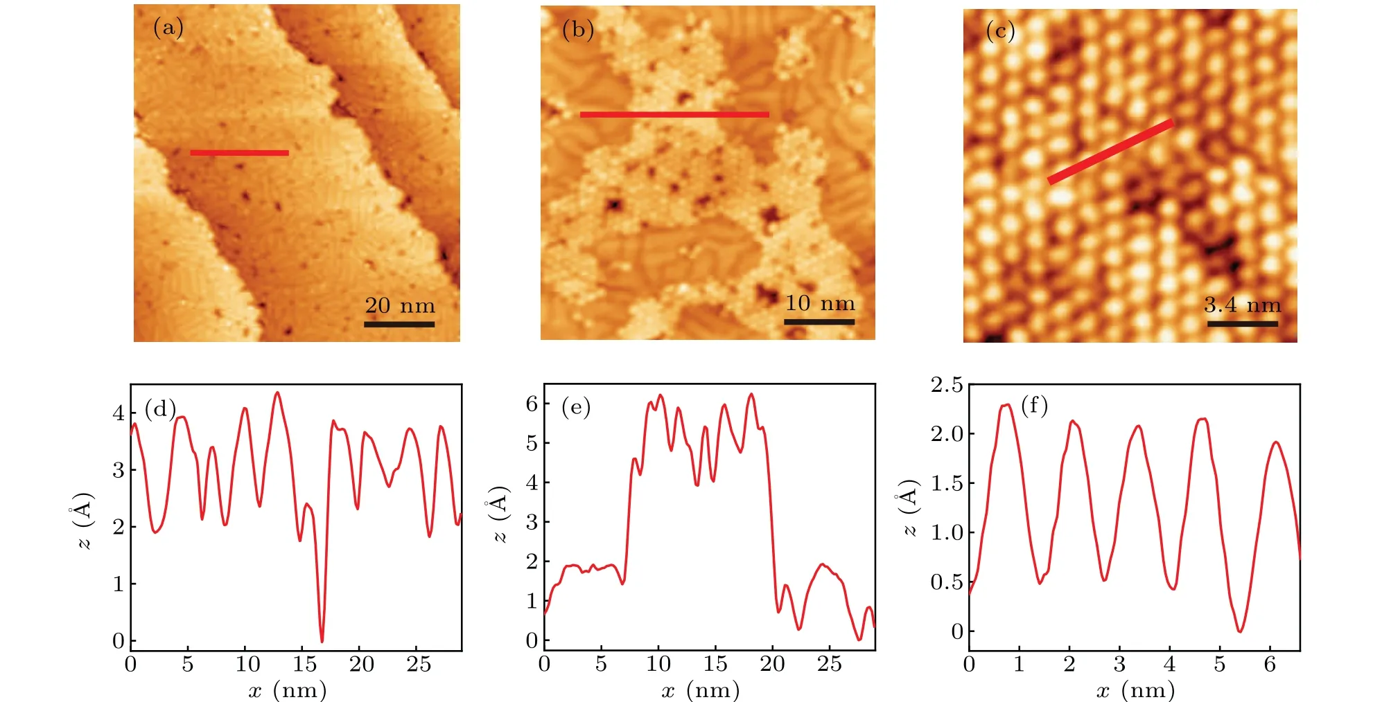
Fig. 1. STM topography images (a)–(c) and corresponding line profiles (d)–(f) of Pb–Si reconstruction surface (a), Sb cluster with coverage of 1.05 ML (b), and hexagonal cluster superlattice (c). Line profiles were taken at the locations marked with red lines in the corresponding STM images. Scan sizes are(a)100 nm×100 nm,(b)50 nm×50 nm,(c)17 nm×17 nm. All tunneling parameters are 1.5 V,100 pA.
Figure 2 presents STM topography images with different Sb coverage at 0.7 ML(Fig.2(a))and 1.05 ML(Fig.2(b)),and the corresponding Sb clusters’ coverages are 18% and 42%,respectively. As shown in Figs. 2(a) and 2(b), the Sb clusters firstly form around the defect sites, and the coverage of clusters increases with the deposition amount increasing. After depositing sufficient amount of 2.8 ML Sb, the surface is approximately fully covered by the Sb clusters and the hexagonal cluster superlattice can be clearly seen as displayed in Fig.2(c).
As mentioned above, antimony as a semimetal element,possesses unique physical properties, which is predicted as a topological insulator with thickness reducing to few layers and realizes the direct observation of the topological edge states.[18–20]Consequently,it is necessary to find an effective method to grow the few layer Sb cluster superlattice for exploring the novel properties. To grow the superlattice, two main pathways are indicated in the past research,i.e.,self-assembly growth and templated growth.[27,28]The templated growth is complicated as a moire pattern film necessary to be grown firstly to serve as the deposition sites before the superlattice growth, while the self-assembly growth only requires a fine adsorption between the evaporated materials and the substrate.Consequently the self-assembly growth is a better choice to grow the superlattice. By growing a buffer layer on the Si substrate and controlling the annealing temperature, we successfully fabricated the two-dimensional self-assembled Sb cluster superlattice. This two-step self-assembly growth method is simple and practicable for fabrication of cluster superlattice,and the two-dimensional Sb cluster superlattice provides a unique platform to explore the novel properties of antimony,such as semiconductor-semimetal transition,topological edge states and quantum spin Hall effect.
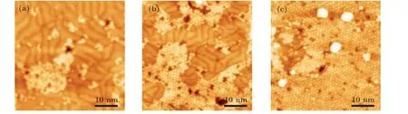
Fig. 2. STM topographies of Sb clusters after deposition (a) 0.7 ML Sb, (b) 1.05 ML Sb, (c) 2.8 ML Sb. All scan sizes are 50 nm×50 nm.Tunneling parameters are(a)1.5 V,100 pA,(b)1.5 V,100 pA,(c)?2.5 V,?100 pA.
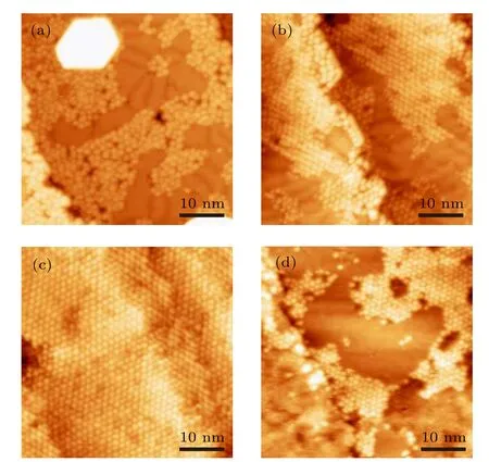
Fig. 3. STM topographies of Sb clusters without annealing (a), after annealing 20 min at 430 K (b), 500 K (c), and 570 K (d). All scan sizes are 45 nm×45 nm. Tunneling parameters are (a) 1.5 V, 100 pA, (b) 1.5 V,100 pA,(c)1.5 V,100 pA,(d)3 V,80 pA.
To uncover the thermal stability of the Sb cluster superlattice,the sample was annealed at different temperatures under ultra-high vacuum(below 7×10?10torr). Figure 3 displays a sequence of STM images of Sb cluster superlattice without annealing(Fig.3(a))and with subsequent annealing for 20 min at 430 K(Fig.3(b)),500 K(Fig.3(c)),and 570 K(Fig.3(d)),respectively. Sb clusters in Fig.3(a)do not form ordered cluster array without annealing. After annealing at 430 K, Sb clusters gain enough kinetic energy to move on the substrate and form hexagonal cluster superlattice with a relative low energy barrier.Compared with the disordered superlattice without annealing(Fig.3(a)),it clearly indicates that the annealing temperature is crucial for the fabrication of the well-ordered superlattice(Fig.3(b)).The Sb clusters fully cover the substrate and the superlattice remains after annealing at 500 K,as shown in Fig.3(c). Further annealing at 570 K results in the destroy of the superlattice and the coverage of the Sb clusters decreases dramatically,indicating that the Sb cluster superlattice is thermally stable up to 500 K.
Up to now, we have indicated the topography and the thermal ability of the Sb cluster superlattice. In order to further explore the detailed atomic structure of the individual Sb nanocluster in the superlattice, high resolution STM measurements were taken on the nanocluster. Figure 4(a) shows an STM topography of Sb cluster superlattice, and the twodimensional Fourier transformation of the cluster superlattice shows clear hexagonal symmetry. Figure 4(b) displays a zoom-in high resolution STM image, which clearly reveals that the Sb clusters in the superlattice consist of different number of Sb atoms ranging from 2 to 7. More specifically,Sb clusters exhibit different shapes, including chain,triangle,rhombus,trapezoid,larger triangle,and combination of rhombus and trapezoid forn=2–7 Sb atoms,respectively,as summarized in Fig.4(c). All the Sb clusters with different shapes show the planar structure. Figure 4(d) displays the statistical distribution of the Sb cluster’s structure where clusters formed byn=3,4,and 5-atoms account for~87%of all structures.It significantly shows that the triangle,rhombus and trapezoid structures of the Sb clusters are more stable comparing to other structures.In addition to the atomic structure study of the nanocluster,another interesting observation is that the growth orientations of clusters are modified by the substrate. As shown in Fig.4(b),4-atom clusters exhibit three orientations with rotation angles of 60?between each other, which is due to the symmetry of the Pb–Si reconstructed surface.

Fig.4. STM images of atomic structure of Sb clusters. (a)High resolution STM topography of Sb cluster superlattice. Inset shows the 2D Fourier transform of Fig.3(a).(b)Zoom-in high resolution STM topography of Sb cluster superlattice. (c)Schematic diagrams of Sb clusters consisting several Sb atoms ranging from 2 to 7. (d)Statistical distribution of the structures of Sb clusters. Scan sizes are(a)15 nm×15 nm,(b)9 nm×9 nm. All tunneling parameters are ?2.5 V,?200 pA.
Lastly, we concentrate on the electronic structure of the Sb cluster by STS measurements. Figure 5(a)depicts the differential conductance (dI/dV) spectra as a function of sample biasVon the adjacent triangular,rhombic and trapezoidal nanoclusters. From the STS measurements,the quantized energy level can be clearly distinguished in the negative bias and the peak-to-peak distance of the triangular, rhombic and trapezoidal nanoclusters is similar(~0.37 eV).We contribute the quantized energy-level to the single-electron tunneling effects. As displayed by Fig.5(b),the tunneling barrier between tip and nanocluster, the tunneling barrier between nanocluster and substrate,can be considered as two capacitors,and the nanocluster in the superlattice can be assumed as an isolated coulomb island due to the weak interaction between the nanoclusters,consequently result in the single-electron tunneling effects. The charge on the nanocluster is accumulated differently for positive and negative bias voltages with the asymmetric double-tunnel barriers.[29]In the positive bias, the transparency for incoming electron is low and that for outgoing electron is high,thus the charge accumulation on the nanocluster is negligible.In the negative bias,the high transparency for incoming electron and low transparency for outgoing electron cause charge accumulation on the nanocluster, which blocks the transport of subsequent single electron. Thus the singleelectron tunneling effects only for negative bias is due to the asymmetric double-tunnel barriers. The lateral sizes of the triangular,rhombic and trapezoidal nanoclusters are close,which leads to the similar capacitance ofC1andC2. Consequently,though the triangular, rhombic and trapezoidal nanoclusters show different structures, their energy spacing between the quantized energy-level is similar.
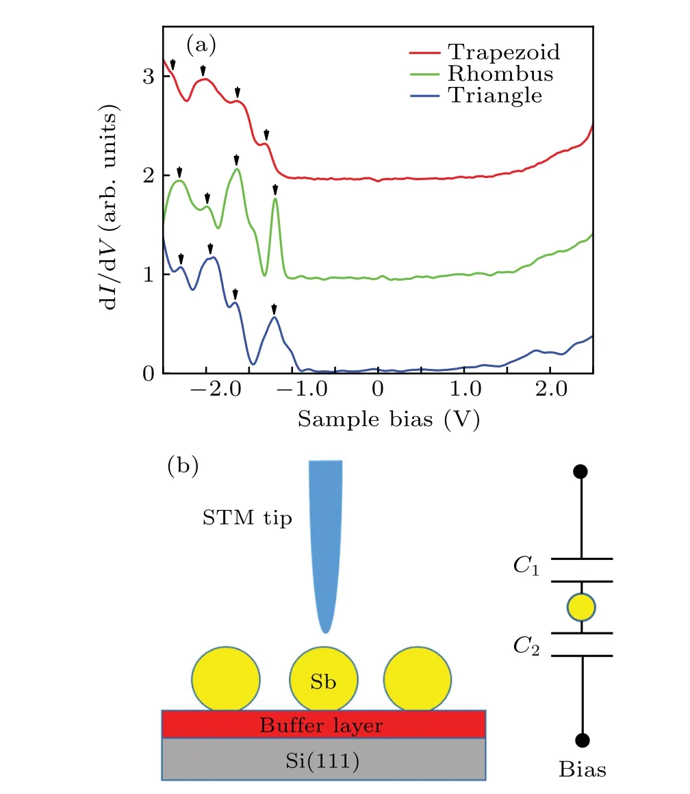
Fig.5. STS measurements of Sb clusters. (a)The differential conductance spectra as a function of sample bias V on the Sb clusters with different structures.(b)Schematic diagram of the double junction,C1 is the capacitor between the STM tip and the Sb cluster,C2 is the capacitor between the Sb cluster and the substrate. All tunneling parameters are?2.5 V,?150 pA.
4. Conclusions
In summary, we have successfully fabricated a twodimensional Sb cluster superlattice by a two-step selfassembly growth method on Si substrate.The two-step growth method provides a simple and practicable pathway for the fabrication of cluster superlattice. More importantly, high resolution STM measurements reveal the fine structures of the Sb clusters in the superlattice, and the triangle, rhombus and trapezoid structures of the Sb clusters are more stable, compared to other structures. Finally, we observe the singleelectron tunneling effects in the cluster superlattice, which provides a promising way to realize the large-scale industrial fabrication of single-electron transistor. We believe that the fabrication of Sb cluster superlattice broadens the species of the cluster superlattice and provides a unique platform to explore the size-dependent properties and the novel quantum phenomena of semimetal nano-materials.
Acknowledgements
Project supported by the National Key Basic Research Program of China (Grant No. 2017YFA0205004),the National Natural Science Foundation of China (Grant Nos. 92165201, 11474261, and 11634011), the Fundamental Research Funds for the Central Universities (Grant Nos. WK3510000006, and WK3430000003), the Anhui Initiative in Quantum Information Technologies (Grant No.AHY170000).
- Chinese Physics B的其它文章
- Magnetic properties of oxides and silicon single crystals
- Non-universal Fermi polaron in quasi two-dimensional quantum gases
- Purification in entanglement distribution with deep quantum neural network
- New insight into the mechanism of DNA polymerase I revealed by single-molecule FRET studies of Klenow fragment
- A 4×4 metal-semiconductor-metal rectangular deep-ultraviolet detector array of Ga2O3 photoconductor with high photo response
- Wake-up effect in Hf0.4Zr0.6O2 ferroelectric thin-film capacitors under a cycling electric field