
Design of vertical diamond Schottky barrier diode with junction terminal extension structure by using the n-Ga2O3/p-diamond heterojunction
2022-10-26 09:54:44WangLin林旺TingTingWang王婷婷QiLiangWang王啟亮XianYiLv呂憲義GenZhuangLi李根壯LiuAnLi李柳暗JinPingAo敖金平andGuangTianZou鄒廣田
Chinese Physics B 2022年10期
Wang Lin(林旺) Ting-Ting Wang(王婷婷) Qi-Liang Wang(王啟亮) Xian-Yi Lv(呂憲義)Gen-Zhuang Li(李根壯) Liu-An Li(李柳暗) Jin-Ping Ao(敖金平) and Guang-Tian Zou(鄒廣田)
1State Key Laboratory of Superhard Material,College of Physics,Jilin University,Changchun 130012,China
2Shenzhen Research Institute,Jilin University,Shenzhen 518057,China
3National Key Discipline Laboratory of Wide Bandgap Semiconductor,Xidian University,Xi’an 710071,China
Keywords: diamond,Schottky barrier diode,junction terminal extension,simulation
1. Introduction
Diamond is a promising material for the next generation power electronic devices because of its low consumption and high-frequency operation. In addition, diamond can be used at high temperature with small leakage current due to its extremely low intrinsic carrier concentration. Compared with conventional power electronic device materials (such as Si, SiC, and GaN), diamond has higher carrier mobilities[4500 cm2/(V·s)for electrons and 3800 cm2/(V·s)for holes],higher critical electric field (>10 MV/cm), higher thermal conductivity[2000 W/(m·K)],lower dielectric constant(5.7),and wide bandgap (5.5 eV).[1,2]The theoretical Baliga figure of merit(BFOM)value of diamond is 23000(normalized to Si), which means that a diamond-based power electronic device is a promising candidate to balance the on-resistance(Ron)and breakdown voltage(VBD).[3,4]
Schottky barrier diodes (SBDs) are the most commonly used electronic component in electric circuits because they have low power loss and no recovery current.[5–10]However,electric field crowding is usually observed in SBDs under a large reverse voltage, which decreases the energy barrier and increases the reverse leakage current seriously. Up to now, various advanced termination structures such as field plates,[11–14]ion implantation,[15–17]and metal guard rings have been adopted to enhanceVBD.[18,19]However, some effective termination structures such as junction terminal extension (JTE) and junction barrier Schottky (JBS) structures are still a challenge for diamond due to the lack of n-type doping.[20]A nitrogen dopant shows a large activation energy of 1.7 eV, whereas a phosphorus dopant shows a low doping efficiency(50%–90%compensation ratio).[21]
Recently, wide bandgap gallium oxide (GaOx) with a bandgap of 4.8 eV and a critical electric field of 8 MV/cm has been adopted to construct n-GaOx/p-diamond heterojunctions.[22]GaOxcan easily obtain n-type doping(1016–1019cm-3) by optimizing the growth conditions,[23]which is beneficial to realizing high-performance photodiodes. In our previous work,[24]the band configuration of the GaOx/diamond interface was determined,which has potential for JTE and JBS application. Herein,a vertical diamond SBD with an n-Ga2O3JTE structure was designed by a Silvaco technology computer-aided design(TCAD)software.By optimizing the JTE length,doping concentration,width,and depth of n-Ga2O3, the trade-off between on-resistance and breakdown voltage without obvious crowding effect on the Schottky contact characteristics was realized.
2. Device structure and simulations
The vertical diamond SBDs with and without n-Ga2O3JTE were designed through Silvaco TCAD. The crosssectional structures of the SBDs are shown in Figs. 1(a)and 1(b). The structure consists of a p+-diamond substrate(1×1019cm-3, 0.5 μm) and a p--diamond drift layer (1×1016cm-3, 3.5 μm). The anode and cathode were located at the bottom and top of the device and set into ohmic and Schottky contact,respectively. For the reference diode without JTE(Fig. 1(a)), the length of the cathode electrode was 10 μm.The n-Ga2O3regions were buried beneath the Schottky contact with an overlap of 1.0 μm.Different n-Ga2O3doping concentrations(1×1017cm-3,5×1017cm-3,1×1018cm-3,and 5×1018cm-3),JTE lengthsL(0 μm,1.5 μm,2 μm,2.5 μm,and 3 μm),and JTE depthsD(0 nm,50 nm,100 nm,150 nm,and 200 nm) were used for the simulations. The commonly used parallel electric field–dependent mobility model, the Auger recombination model,the Shockley–Read–Hall model,and the impact ionization model were adopted to obtain the current–voltage (I–V) curve and electric field distribution of the SBDs.[25]In addition,a universal phonon-assisted tunneling model was defined at the anode region. The key material parameters of diamond and Ga2O3[26]in the simulations are shown in Table 1. The electron mobilityμn(hole mobilityμp)of p+diamond,p-diamond,and n-Ga2O3were 1000(30)cm2/(V·s),1000(200)cm2/(V·s),and 200(50)cm2/(V·s),respectively. The impact ionization parameters of diamond and Ga2O3are shown in Table 2.

Table 1. Key material parameters of diamond and Ga2O3 used in the simulations.
Table 2. Impact ionization coefficients of diamond[27] and Ga2O3 used in the simulations.[28]
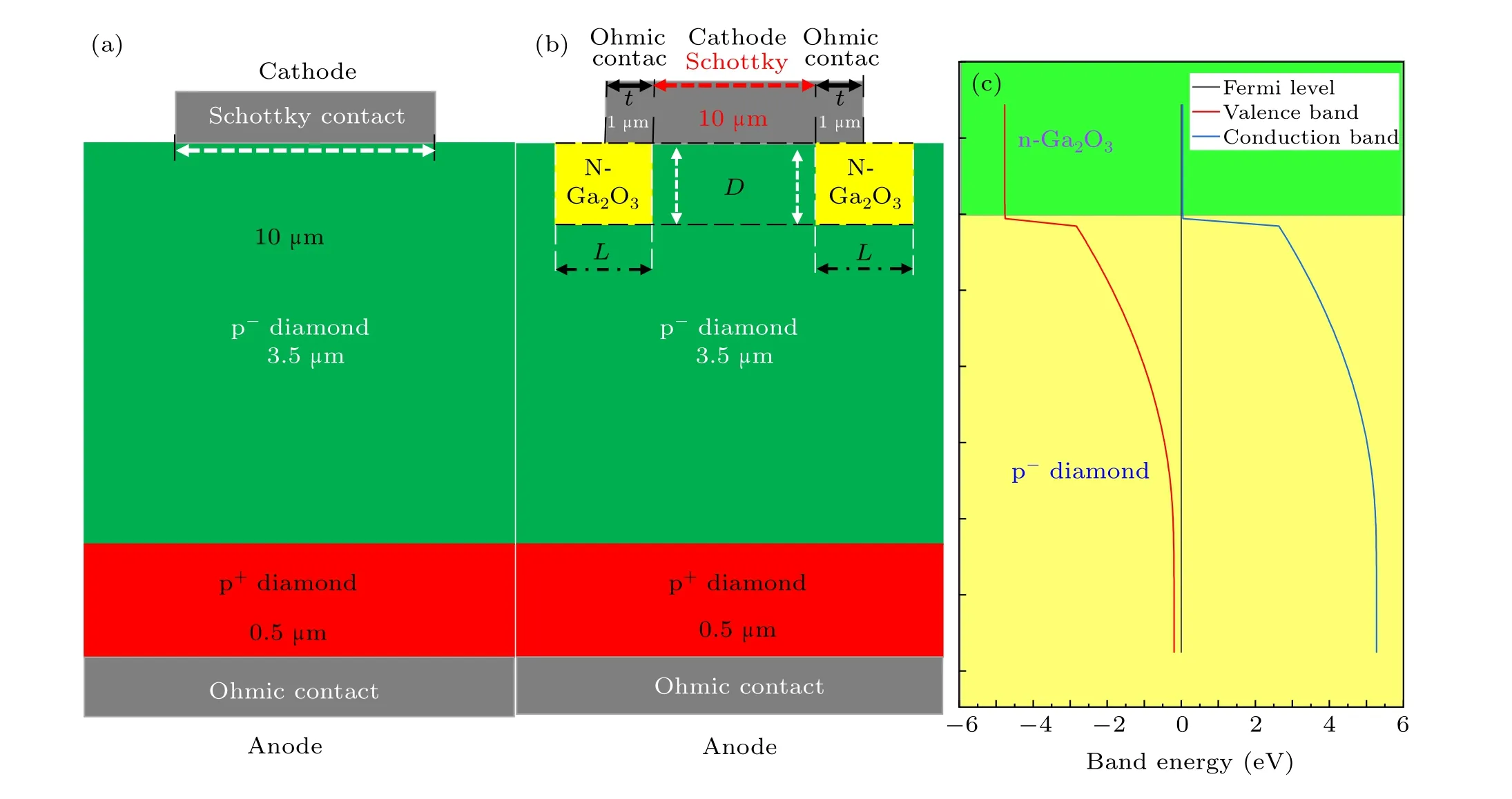
Fig.1. Schematic structures of the vertical diamond SBDs(a)without and(b)with n-Ga2O3 JTE;(c)energy band diagram along the heterojunction interface with the doping concentrations of Ga2O3 and diamond being 1×1018 cm-3 and 1×1016 cm-3,respectively.
3. Results and discussion
3.1. Effect of n-Ga2O3 JTE on the electrical properties
The depletion region introduced by the n-Ga2O3/pdiamond heterojunction plays a key role in the device performance. First, an n-Ga2O3doping concentration of 1×1018cm-3and a JTE length of 3.5 μm were chosen for the simulation. Depths of 50 nm, 100 nm, 150 nm, and 200 nm were adopted for comparison with the diode without JTE(0 nm). The simulated electrical characteristics are shown in Table 3. The obtainedI–Vcurves of the SBDs with different JTE lengths are shown in Fig. 2(a). When compared with the reference diode (0 nm), the turn-on voltages (Von)are comparable for all the SBDs. However, the current density decreases obviously due to increasingRon(Table 3). On the basis of the forward current distributions in Fig.3,the depletion region in n-Ga2O3suppresses the conduction path and increases the total diode area, resulting in the increase ofRonfrom 0.97 mΩ·cm2to 1.68 mΩ·cm2(Table 3).
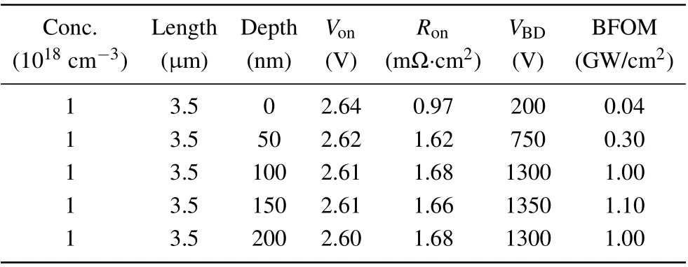
Table 3. Simulated electrical characteristics of the SBDs with different JTE depths.
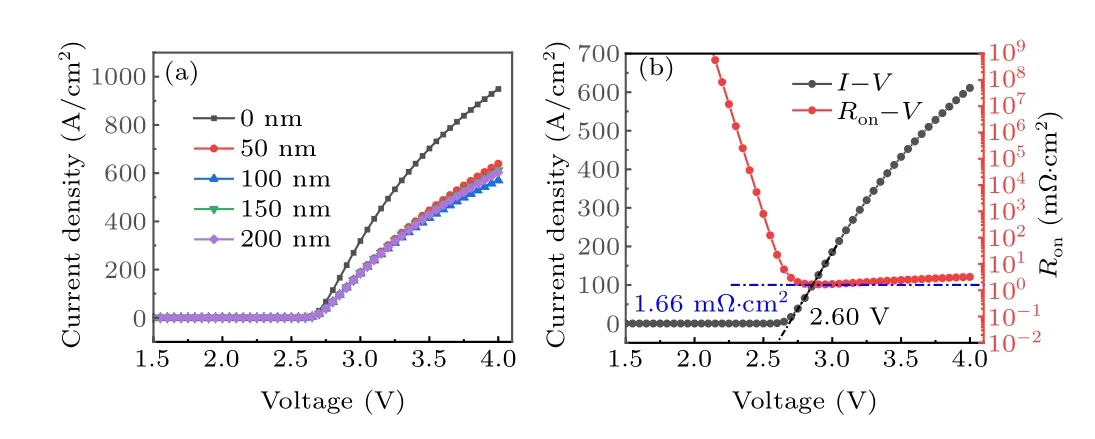
Fig.2. (a)The I–V curves of the SBDs with different Ga2O3 depths;(b)typical I–V curve and the corresponding Ron for an n-Ga2O3 depth of 150 nm.
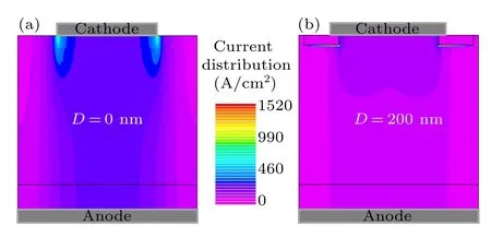
Fig. 3. Current distributions of the vertical diamond SBDs (a) without and(b)with 200-nm n-Ga2O3 JTE under a forward bias of 3 V.
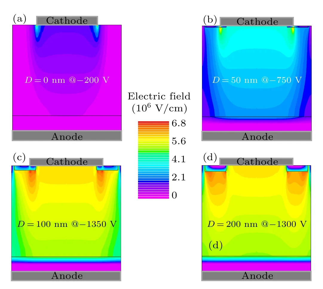
Fig.4. Electric field distributions under VBD for the vertical diamond SBDs with JTE depths of(a)0 nm,(b)50 nm,(c)150 nm,and(d)200 nm.
From Table 3, theRonvalues of the SBDs with different depths of n-Ga2O3are comparable to each other butVBD(the electric field reaches 6 MV/cm) first increases and then decreases with increasing depth. The highestVBDand BFOM value are 1350 V and 1.10 GW/cm2for the SBD with a JTE depth of 150 nm. From the electric field distribution atVBD,obvious crowding effect occurs at the edge of the electrode for the SBD without JTE(Fig.4(a)). After the introduction of JTE,the depletion regions in n-Ga2O3and p-diamond sustain the reverse bias. Then, the electric field is distributed more even and broader, which is beneficial to realizing higherVBD(Figs.4(b)and 4(c)). However,the electric field tends to concentrate beneath n-Ga2O3with the peak field occurring at the edge of JTE when the depth increases to 200 nm,resulting in the decrease ofVBD(Fig. 4(d)). The variation in the electric field distribution is also confirmed from the profiles shown in Fig.5.
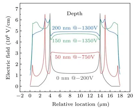
Fig.5. Electric field profiles under VBD for the vertical diamond SBDs with JTE depths of 0 nm,50 nm,150 nm,and 200 nm.
3.2. Optimization of the doping concentration of n-Ga2O3
To search the best doping concentration of n-Ga2O3, the effect of doping concentration on the electrical characteristics is studied. Doping concentrations of n-Ga2O3of 1×1017cm-3,5×1017cm-3,1×1018cm-3,and 5×1018cm-3were selected with the depth and length of n-Ga2O3being 150 nm and 2.5 μm, respectively. The simulation results are shown in Table 4.
Figure 6(a) shows the forward-biasedI–Vcurves of the SBDs with different doping concentrations of n-Ga2O3. The figure demonstrates that the current densities andVonvalues are comparable for all the SBDs, implying that the forward conduction is determined by the Schottky contact.TheVonandRonof the SBDs are deduced from theI–Vcurves and summarized in Table 4. By taking the SBD with a doping concentration of 1×1018cm-3as an example (Fig. 6(b)),Vondefined by a linear extrapolation method andRonwere calculated to be approximately 2.61 V and 1.47 mΩ·cm2, respectively. From Table 4, although all theVonvalues of the SBDs are nearly the same,Ronincreases slightly with increasing doping concentration. The mechanism can be explained from the forward current distributions as shown in Fig.7. The depletion region at the n-Ga2O3/p-diamond interface is widened at higher doping concentration,which will suppress the conduction area and increaseRonslightly. On the basis of the aforementioned results,1×1018cm-3was chosen as the optimum concentration to obtain the highest BFOM value.
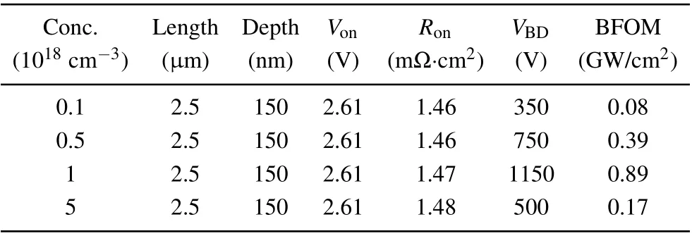
Table 4. Simulated results for the SBDs with different doping concentrations of n-Ga2O3.

Fig.6. (a)The I–V curves of the SBDs with different doping concentrations of n-Ga2O3; (b) typical I–V curve and the corresponding Ron for a doping concentration of 1×1018 cm-3.
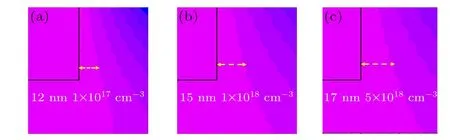
Fig.7.Depletion region width at the junction interface under different doping concentrations of n-Ga2O3.

Fig.8. Electric field distributions under VBD for the vertical diamond SBDs with doping concentrations of (a) 1×1017 cm-3, (b) 5×1017 cm-3, (c)1×1018 cm-3,and(d)5×1018 cm-3.
The variation inVBDversus the doping concentration was also evaluated, as shown in Fig. 8. The figure demonstrates that the n-Ga2O3layer is totally depleted at the edge of the cathode when the doping concentration is 1×1017cm-3, resulting in a relatively lowVBD. The depletion region with a high doping concentration extends the electric field distribution and separates the peak into two parts, namely the edges of n-Ga2O3and the cathode electrode. However,the dominant electric field peak shifts to the edge of n-Ga2O3for a doping concentration of 5×1018cm-3. This can be attributed to the depletion region in n-Ga2O3being too narrow to sustain the reverse voltage. The variation in the electric field distribution is also confirmed from the profiles shown in Fig.9.
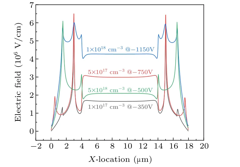
Fig.9. Electric field profiles under VBD for the vertical diamond SBDs with different doping concentrations of n-Ga2O3.
3.3. Optimization of the JTE length
Here, a doping concentration of 1×1018cm-3and a depth of 150 nm are chosen to evaluate the effect of JTE length on the device performance.The simulated electrical characteristics are summarized in Table 5,and the obtainedI–Vcurves of the SBDs with different JTE lengths are shown in Fig.10(a).It demonstrates that theVonvalues are comparable for all the SBDs, whereas the current density decreases with increasing length. The introduction of JTE increases the total diode area and then increasesRonfrom 0.97 mΩ·cm2to 1.66 mΩ·cm2(Table 5).

Table 5. Simulated electrical characteristics of the SBDs with different JTE lengths.
On the other hand, it can be observed that the reverseVBDincreases from approximately 200 V to 1350 V when the length increases to 3.5 μm. The calculated BFOM values presents a maximum of 1.10 GW/cm2for the SBD with a JTE length of 3.5 μm. The electric field distribution under the reverse bias region is also simulated to determine the mechanism of the JTE length (Fig. 11). When the doping concentration in the JTE is 1×1018cm-3, the depletion regions in both Ga2O3and diamond sustain the reverse bias. Therefore,the electric field distribution is extended with increasing JTE length,resulting in enhancedVBD.

Fig. 10. (a) The I–V curves of the SBDs with different JTE lengths; (b)typical I–V curve and the corresponding Ron for a length of 3.5 μm.
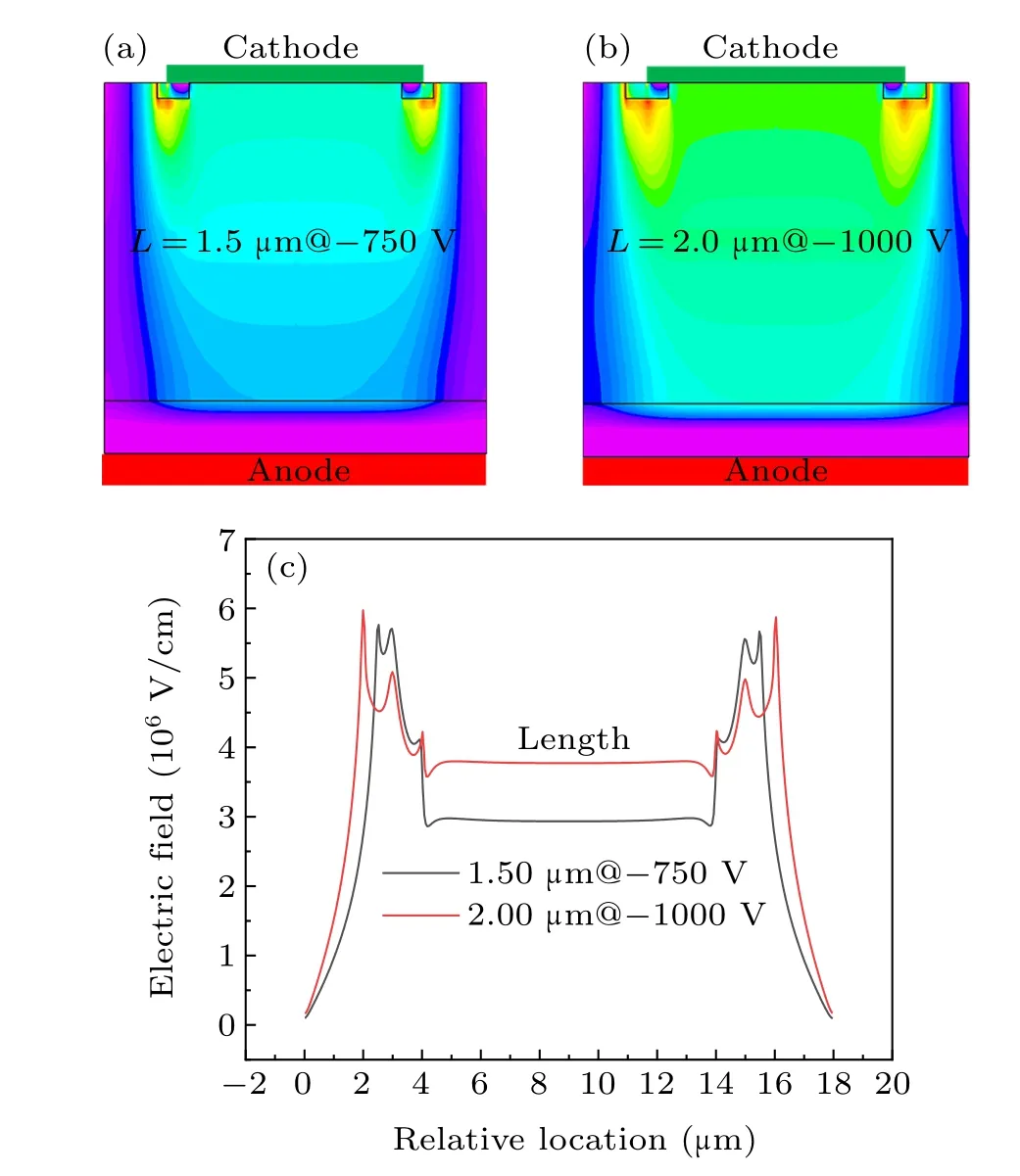
Fig. 11. [(a), (b)] Electric field distributions and (c) profiles under VBD for the vertical diamond SBDs with JTE lengths of 1.5 μm and 2.0 μm.
3.4. Effect of work functions of the Schottky electrodes
On the basis of the prior discussion,the optimum length,depth, and doping concentration of the n-Ga2O3region have been obtained.However,theVonof the diode is relatively high,which requires a trade-off betweenVonandVBD. Generally,Vonpresents a direct relationship with Schottky barrier height,which can be effectively modulated by a work function. Different cathode electrode materials(work functions)are chosen for further evaluation. The corresponding electrical characteristics are summarized in Table 6.The electrode material(work functions) has no obvious effect onVBD. By considering the material properties, cost, and device parameters given in Table 6, we think that Al and Cu are the preferable electrode materials,which are also compatible with the conventional Si CMOS process.

Table 6. Simulated electrical characteristics of the SBDs with different Schottky electrode materials.
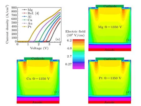
Fig. 12. (a) The I–V curves of the SBDs with different Schottky electrode materials;electric field distributions of(b)Mg,(c)Cu,and(d)Pt at a reverse voltage of 1350 V.
4. Conclusions and perspectives
Vertical diamond SBDs with and without an n-Ga2O3JTE structure were proposed and simulated by Silvaco TCAD.The introduction of n-Ga2O3JTE decreases the forward current density while enhancing the reverse breakdown voltage effectively with a medium depth of 150 nm. In addition,Ronincreases slightly with increasing doping concentration of n-Ga2O3while the electric field is distributed more even and broader. However,the depletion region in n-Ga2O3is too narrow to sustain the reverse voltage when the doping concentration is higher than 5×1018cm-3. Furthermore,the electrical characteristics of the SBD can be enhanced with a large JTE length but with the increasing device area. Finally,Al and Cu were chosen as the preferable electrode materials to balance the forward turn-on voltage and the reverse breakdown voltage.
Acknowledgments
Project supported by the Key Research and Development Program of Guangdong Province, China (Grant No. 2020B0101690001) and the Natural Science Foundation of Sichuan Province,China(Grant No.2022NSFSC0886).
- Chinese Physics B的其它文章
- Multiple modes of perpendicular magnetization switching scheme in single spin–orbit torque device
- Evolution of the high-field-side radiation belts during the neon seeding plasma discharge in EAST tokamak
- Phase-matched second-harmonic generation in hybrid polymer-LN waveguides
- Circular dichroism spectra of α-lactose molecular measured by terahertz time-domain spectroscopy
- Recombination-induced voltage-dependent photocurrent collection loss in CdTe thin film solar cell
- Development of ZnTe film with high copper doping efficiency for solar cells