Electronic states of domain walls in commensurate charge density wave ground state and mosaic phase in 1T-TaS2
2023-09-05 08:48:24YanLi李彥YaoXiao肖遙QiZheng鄭琦XiaoLin林曉LiHuang黃立andHongJunGao高鴻鈞
Chinese Physics B 2023年7期
Yan Li(李彥), Yao Xiao(肖遙), Qi Zheng(鄭琦), Xiao Lin(林曉),Li Huang(黃立),?, and Hong-Jun Gao(高鴻鈞)
1Beijing National Center for Condensed Matter Physics and Institute of Physics,Chinese Academy of Sciences,Beijing 100190,China
2School of Physical Sciences,University of Chinese Academy of Sciences,Beijing 100490,China
Keywords: 1T-TaS2,scanning tunneling spectroscopy,domain walls,charge density wave
Domain walls (DWs) in 1T-TaS2have great influences on the electronic properties of the material,[1–10]thus have always been one of the key research directions in this field.Although the strength of the electron–electron correlation is similar inside the intrinsic 1T-TaS2domains, the correlation strength decreases where DWs exist.[6]The interplay between charge density wave (CDW) and electron correlation renders rich physics in the electronic states of DWs.[1–3,6,11,12]
Intensive experimental and theoretical studies have demonstrated that DWs with different atomic structures have different electronic states, ranging from insulating to conductive.[3,6,13,14]Furthermore,the density of DWs also affects the electronic states of the system.[6,15]For example,1T-TaS2will change from a Mott insulator in commensurate CDW (CCDW) phase to a metal when the density of DWs increases significantly.[14,16,17]In the CCDW phase, a voltage pulse across the tip–sample junction could create DWs in high density,resulting in a mosaic state that can be metallic.[2]Therefore, the electronic states of DWs are not only determined by the atomic structures,but also by the density of the DWs.The complexity of this hinders the understanding of the electronic states in DWs,which calls for more thorough work to investigate DWs of different types in different densities.
Here, we present the scanning tunneling spectroscopy(STS) results on the DWs of 1T-TaS2in areas with different DW densities, namely DWs between large CCDW domains,between a large and a small CCDW domain, and in the mosaic phase.We found that for DWs between large domains,the STS on both DWs and the domain edges(DEs),the nearest intact stars of David (SDs) on the two sides of the DWs have a V-shaped gap with no spectral weight atEF.For DWs between a large and a small CCDW domain, the DEs have a finite spectral weight atEF, indicating a metallic state, while the DWs remain insulating.For DWs in the mosaic phase,the domains can be metallic or insulating.The electronic states on the domain edges and inside the domains tend to have the same states.The DWs show states suppression nearEFand share some similar states with the domains.
Our scanning tunneling microscopy/spectroscopy(STM/S) measurements were carried out in a Createc STM system in ultrahigh vacuum condition, with a base pressure better than 5×10?1mbar,at a low-temperature of 4.3 K.The 1T-TaS2single crystal was purchased from HQ Graphene.The samples with pre-glued aluminum rods were cleaved at room temperature in the UHV chamber, and then transferred to the precooled STM head immediately.STM images were acquired in the constant current mode.
The 1T-TaS2has a commensurate charge density wave(CCDW)ground state when the temperature is below 180 K,in which the triangular-latticed Ta atoms deform into SDs where every 12 Ta atoms contract towards a central Ta site,forming asuperlattice[18–21](Fig.1(a)).The CCDW superstructure is accompanied by electronic modulations, leaving only one conduction electron per SDs.[22–26]Strong electron correlations between SD clusters further lead to a Mott insulating ground state.[27–32]The SDs have shifted center positions in different domains.The merge of two domains results in a domain wall(DW)that consists of one or two incomplete lines of SDs.[1,13]Judging from the atomic structure,there are 12 possible types of DWs, each of which possesses unique electronic structures.[3,13]In the CCDW phase, DWs usually locate between large-are domains (Fig.1(b)).While in the mosaic phase,the DWs have high density,resulting in domains with very small areas(Fig.1(c)).
Figure 2(a) shows an STM image of the CCDW region with a DW marked by two parallel black dashed lines.The domains (marked by D) have triangular-latticed SDs, while the DW has a much lower contrast in the STM image at this scanning parameter.DWs in 1T-TaS2can be classified into 12 types,out of which only 3 types of DWs,DW1,DW2 and DW4, have high frequency of occurrence,[6,13]as shown by the STM images in Figs.2(b)–2(d), respectively.The superimposed lilac and pink SD models illustrate the relative shifts of the SD centers in the neighboring domains.Among the three DWs,DW1 and DW4 consist of only one column of incomplete SDs, while DW2 is composed of two columns of incomplete SDs,as indicated by the black dashed lines in each figure.The DEs, which are the nearest complete SDs on the two sides of the DWs, are highlighted by the white dashed lines.
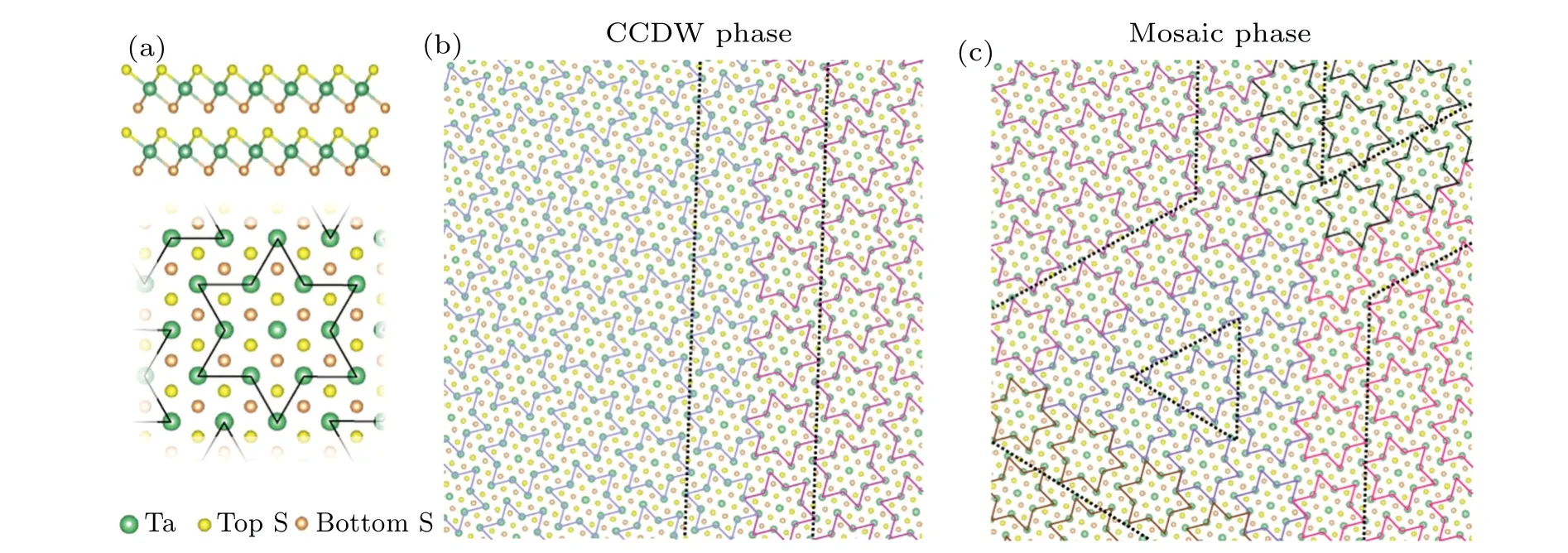
Fig.1.Schematic of atomic structure of 1T-TaS2.(a)Side view and top-view atomic structure of 1T-TaS2.The superimposed black lines show the SD.(b) The atomic structure of DW in the CCDW phase.The two domains are superimposed with lilac and pink SD superlattices.The DW is marked by two parallel black dashed lines.(c)The atomic structure of DWs in the mosaic phase.Different domains are superimposed with SD superlattices with different colors.The DWs are marked by parallel black dashed lines.
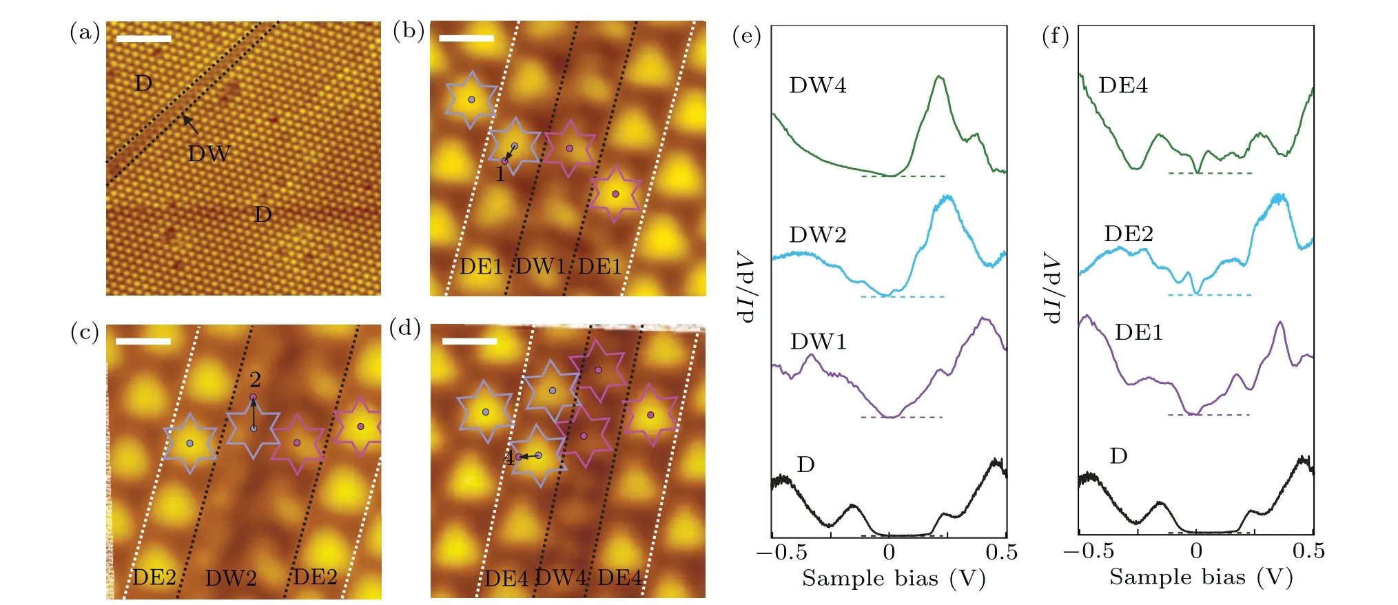
Fig.2.STM images and STS on DWs between large domains in 1T-TaS2.(a)Large-area STM image of CCDW domains and a DW in the upper left part of the image.The black dashed lines highlight the position of the DW.(b)–(d)Zoom-in STM images of DW1,DW2,DW4,superimposed with the schematic lilac and pink DS superlattice.Domain walls with deformed SDs are marked by dashed black lines.Domain edges with complete SDs nearest to the DWs on both sides are drawn out by the white dashed lines.The black arrows show the vectors of the relative phase shifts of the CDW pattern between the two domains.(e) dI/dV spectra taken on the CCDW domain region(black),DW1(purple),DW2(blue)and DW4(green).The horizontal dashed lines represent the zero spectral weight of each STS.The STS curves are vertically shifted for clarity.(f) dI/dV spectra taken on the CCDW domain region(black),DE1(purple),DE2(blue)and DE4(green).STM scanning parameters in(a)–(d):bias voltage applied to the sample VS=?1 V,tunneling current It=10 pA.STS parameters in(e)and(f): VS =?0.1 V,It =10 pA,the modulated output voltage from the lock-in amplifier Vmod =5 mV,modulation frequency fmod =761 Hz.Scale bars: 8 nm in(a)and 1 nm in(b)–(d).
The dI/dVspectra taken on both DWs and DEs in Figs.2(e)and 2(f)show a V-shaped gap instead of a Mott gap around the Fermi level.The incomplete SDs in DWs are accompanied by the changes of the onsite Coulomb repulsion energyU,therefore reduce the width of the Mott gap.[6,8]Once breaking the long range CDW order, the Mott gap of DWs turns into a V-shaped gap,because the peaks corresponding to the upper Hubbard band(UHB)and the lower Hubbard band(LHB) become broader and closer to the Fermi level.For all the DWs and DEs in Fig.2, the spectral weight at the Fermi level is zero.The dI/dVspectra taken at the second nearest SD neighbors to the DWs returns to a normal Mott gap, indicating that the electronic states of these SDs are no longer subject to the influence of DWs.
In the DW regions,the incomplete SDs can no longer trap the unpaired 5d electrons at the center of SD, which leads to the weakening of Coulomb interaction together with increasing of electron hopping between adjacent SDs.Therefore,the lower Hubbard band and the upper Hubbard band shift towards the Fermi level,resulting in Mott collapse with a V-shaped gap on the DWs.For the DE regions,although the SDs are intact,they are still affected by the delocalized 5d electrons in the DW regions, rendering a similar V-shaped gap as that on the DWs.
Next, we created a mosaic phase by applying voltage pulses from the STM tip.[1,2,4]Since the periodicity is significantly broken in the mosaic region, the electronic states of DWs and domains can be fairly complicated.[1,2,4,9]We first focus on the edge area of the mosaic region, where the DWs are relatively sparse,as shown in the large-area STM image in Fig.3(a).The black dashed lines mark the edges of a large domain(DL)and a triangular shaped small domain(DS),which are separated by a DW2.The zoom-in STM image in Fig.3(b)shows the DW2 (marked by the parallel black dashed lines),the domain edges to the DLand DSside (DELand DES, by white dashed lines),and the two domains.
The DLhas similar electronic states as those in large-area CCDW domains, as shown by the pink curve in Fig.3(c).However, the STS of DShas a metallic V-shape around the Fermi level (green curve in Fig.3(c)), which is a feature for small domains in the mosaic region due to the reduction of electron correlation as reported by published works.[1,2]Furthermore, there are additional free electrons released by the Mott collapse to make the metallic state, indicating the electron correlation in DSshould be even weaker than that in the DWs in large-area CCDW regions as shown in Fig.2.Similar to the STS of DW2 in Fig.2,there is also a V-shaped gap in the dI/dVspectra of DW2 in Fig.3(c) (the red curve), whereas the states at the unoccupied energies look very different.For the domain edges though,the STS on both DELand DEShave a V-shape with finite spectral weight around the Fermi level,which is different from the case in large-area CCDW where the DE2 is insulating.The higher density of domain walls leads to weaker electronic correlations compared to the largearea CCDW regions, resulting in more delocalized 5d electrons contributing to the metallic state on the domain edges.
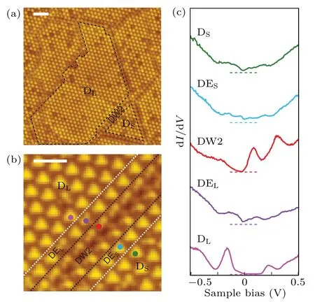
Fig.3.STM images and STS on DW2 in a mosaic region with relatively sparse DWs in 1T-TaS2.(a) Large-area STM image of an area composed of mosaic domains separated by sparse domain walls.Superimposed black dashed lines enclose two typical domains.(b) Zoom-in STM image of the same DW2 as highlighted in(a).DW2 is circled by the parallel black dashed lines.Domain edges with complete SDs nearest to the deformation SDs on both sides are drawn out by the white dashed lines.The colorful circles mark the positions where dI/dV spectra are taken.(c) dI/dV spectra taken at DL(pink), DS (green), the domain edge near the large domain (DEL, purple),the domain edge near the small domain (DES, blue) and DW2 (red).The horizontal dashed lines represent zero spectral weight of each STS.The STS curves are vertically shifted for clarity.STM scanning parameters in(a)and(b):VS=?1 V,It=10 pA.STS parameters in(c):VS=?0.1 V,It=10 pA,Vmod=5 mV, fmod=761 Hz.Scale bars: 5 nm in(a)and 2.5 nm in(b).
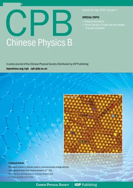
For the mosaic region with intensive DWs,the long-range ordered CCDW pattern is divided into small pieces of polygons separated by DWs, as shown by the black dashed lines in Fig.4(a).We have performed STS characterizations on multiple DWs and domains.For domains, the electron states are V-shaped, like the ones on the DWs or DEs in the largearea CCDW region.We noticed that the spectral weight at the Fermi level varies in different domains.For example,the light blue curve(domain D)in Fig.4(b)is insulating,while the dark blue curve(domain D′)is metallic.Some published works indicate that dense DWs not only change the localized Coulomb repulsion, but also change the bandwidth.[7,33–36]Also, the vertical stacking orders of different domains may contribute to the varied electronic states.[4,35]
The STS taken at DW1, DW2,8, and DW4 all display a V-shape feature(the green,red and purple curves in Fig.4(b)),among which DW4 has more spectral weight at the Fermi level,whereas the other DWs have near zero conductance near the Fermi level.What’s more, the spectra taken at both DWs and domains of the mosaic region seem to share some similar states at?40 meV,+50 meV and+200 meV,as indicated by the orange dotted vertical lines in Fig.4(b),although the relative intensity of these peaks varies on different sites.Therefore, we can infer that in the mosaic area, the influence of breaking the long-range CDW order spreads from the original one or two columns of DW SDs to the entire mosaic region.
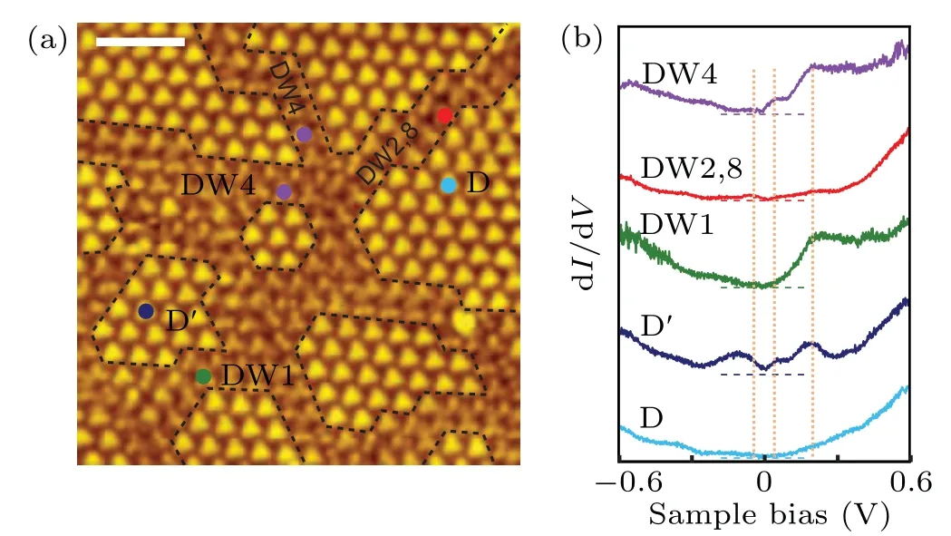
Fig.4.STM image and STS on DWs in a mosaic region in 1T-TaS2.(a)STM image of mosaic domains separated by dense DWs.The black dashed lines show the edges of the domains.The types of DWs are marked in the figure.The colorful circles show the positions where the dI/dV spectra were taken.(b) dI/dV spectra taken in domains(light blue and dark blue),DW1(green),DW2,8 (red) and DW4 (purple).The horizontal dashed lines represent zero spectral weight of each STS,while the vertical dotted orange lines mark peaks shared by several STS.The STS curves are vertically shifted for clarity.STM scanning parameters in (a): VS =?1 V, It =10 pA.STS parameters in (b):VS=?0.1 V,It=10 pA,Vmod=5 meV, fmod=761 Hz.Scale bar: 4 nm.
Compared with previous works on mosaic phase in which the whole region shows a metallic state,[1,2]our work discovers that there are also insulating regions both within domains and on DWs in the mosaic phase.With the high density of DWs,the delocalization of 5d electrons in the DWs has strong influence on the intact SDs,resulting in a complete Mott collapse not only on DWs and DEs,but also within the domains.Some studies suggest that the additional free electrons released by Mott collapse may form quasi-particle energy bands that split into bonding and anti-bonding states,[6]which may be a possible reason for the insulating areas in the mosaic phase observed in this work.However,due to the complexity of the type of DWs and the size of domains, further investigations are still needed to elucidate the mechanism for the electronic states in the mosaic phase.
In conclusion, we demonstrated that the large-area CCDW phase in1T-TaS2has a zero conductance around the Fermi level both in domains and at DW1,DW2,DW4 and their DEs.However,in the mosaic region,the electronic states are very complicated.Besides the shared feature of a V-shaped spectra around the Fermi level, the domains, DWs, and DEs can be metallic or insulating,which seem to be highly affected by the neighboring environment.Our work provides detailed information on the electronic states in both large-area CCDW and mosaic phases,which may contribute to better understanding of the interplay of CDW and electron correlations in1TTaS2.
Acknowledgements
Project supported by the National Key Research and Development Project of China (Grant No.2019YFA0308500),the National Natural Science Foundation of China (Grant No.61888102),and the Chinese Academy of Sciences(Grant Nos.XDB30000000 and YSBR-003).
- Chinese Physics B的其它文章
- First-principles calculations of high pressure and temperature properties of Fe7C3
- Monte Carlo calculation of the exposure of Chinese female astronauts to earth’s trapped radiation on board the Chinese Space Station
- Optimization of communication topology for persistent formation in case of communication faults
- Energy conversion materials for the space solar power station
- Stability of connected and automated vehicles platoon considering communications failures
- Lightweight and highly robust memristor-based hybrid neural networks for electroencephalogram signal processing