NiO/β-Ga2O3 heterojunction diodes with ultra-low leakage current below 10-10 A and high thermostability
2023-10-11 07:56:32YiHuang黃義WenYang楊穩QiWang王琦ShengGao高升WeiZhongChen陳偉中XiaoShengTang唐孝生HongShengZhang張紅升andBinLiu劉斌
Chinese Physics B 2023年9期
Yi Huang(黃義), Wen Yang(楊穩), Qi Wang(王琦),?, Sheng Gao(高升), Wei-Zhong Chen(陳偉中),Xiao-Sheng Tang(唐孝生), Hong-Sheng Zhang(張紅升), and Bin Liu(劉斌)
1School of Optoelectronic Engineering,Chongqing University of Posts and Telecommunications,Chongqing 400065,China
2School of Electronic Science and Engineering,Nanjing University,Nanjing 210093,China
Keywords: NiO/β-Ga2O3 p–n heterojunction diodes, Baliga’s figure of merit, reverse leakage current, β-Ga2O3 power devices
1.Introduction
Beta-phase gallium oxide(β-Ga2O3)shows great potential as a high-power device material.It is predicted to become a research hotspot for the next generation due to its ultrawide bandgap and high critical electric field (8 MV/cm), superior to SiC and GaN.[1–4]The unipolar- and bipolar-power devices based onβ-Ga2O3have high application value in electronic circuits.[5]One notable potential market is in the applications of power converters, inverters, and power supplies for servers.[6–8]However,the difficulty in realizing p-typeβ-Ga2O3is still an obstacle to realizing advanced bipolar power devices in practical applications.It could be an alternative choice to construct heterojunctions by employing other p-type oxide materials onβ-Ga2O3.[5,9]In the p-type oxide family,wide bandgap NiO materials can be used for integration with n-Ga2O3due to their high-visible spectral transparency and p-type conductivity derived from nickel vacancies or monovalent impurities.[10]Heet al.successfully achieved selective high-resistance zones onβ-Ga2O3wafers,which considerably reduced the leakage current and increased the breakdown voltage of Schottky barrier diodes(SBD).[11]Xionget al.reported aβ-Ga2O3double-barrier Schottky barrier diode (DBSBD)with a low turn-on voltage of 1.13 V and low reverse leakage current of 1.27×10⁻⁷A/cm2(at-100 V).[12]Recently,NiO/Ga2O3HJDs have been proven to have excellent reverse blocking ability.Luet al.reported a vertical NiO/β-Ga2O3heterojunction diode by sputtering a layer of NiO thin film onβ-Ga2O3substrate,and its breakdown voltage(VBR)exceeded 1 kV.[13]Xuet al.demonstrated an effective edge termination for vertical NiO/β-Ga2O3heterojunction diodes using a continuous p-NiO film as a junction termination extension(JTE),which increased theIon/Ioffratio up to~1010A and achieved a high breakdown voltage of 2.66 kV.[14]Gonget al.reported a double-layered NiO/β-Ga2O3p–n heterojunction diode and obtained a 1.86 kV high breakdown voltage(BV)and low reverse leakage current below 1 μA/cm2.[10]In recent years,NiO/β-Ga2O3HJDs have achieved a high breakdown voltage of nearly 2 kV, but most of them have high reverse leakage current under high reverse bias voltage.And the changes in electrical properties such as voltage,on-resistance and reverse leakage current of various devices under high temperature and variable temperature still need further study.
In this work, the NiO/β-Ga2O3HJDs are prepared with 10 nm thick p-NiO prepared by thermal oxidation of Ni on theβ-Ga2O3.The breakdown voltage is as high as 465 V,and excellent forward and reverse output characteristics are obtained.The output characteristics of the HJDs under different temperatures are tested.It is found that the reverse leakage current of the HJDs is basically unchanged and the variation range is between 10-11–10-10A.Meanwhile,the leakage current can be maintained below 10-10A, and the high-temperature resistance of the devices is excellent.This paper, thus, further confirms the potential of Ga2O3HJDs for high power, high temperature,and high-reliability applications.[15–17]
2.Device fundamentals
Figure 1(a) shows a schematic cross-section of a vertical NiO/β-Ga2O3HJD on a highly conductive Sn-doped(001)β-Ga2O3substrate with an electron concentration of 1.5×1019cm-3.The 6 μm Si-dopedβ-Ga2O3drift region was grown by hydride vapor phase epitaxy.The doping concentration was measured by Hall measurement at room temperature to be 2×1016cm-3.Firstly, the 30/150 nm Ti/Au was deposited by electron beam evaporation to form a backside ohmic contact (cathode), followed by rapid thermal annealing at 480°C for 1 min under a N2ambient.After the lithography,the metal Ni was evaporated at the heterojunction in the drift region,followed by oxidation at 400°C for 20 min.The Ni was oxidized to create 10 nm thick NiO to form a p-NiO layer.The thickness of the p-type NiO is measured by atomic force microscope.The Hall measurement characterizations of the p-NiO film indicate that the 10-nm-thick layer has hole concentrations of 1.33×1018cm-3.Finally,a Ni/Au(200/150 nm)layer was deposited on the NiO layer as a metal anode.Meanwhile, the Ni/β-Ga2O3SBD was also manufactured on the same chip using identical processes.Figure 1(b)is the SEM anode surface image of the HJD,and the diameter of the metal anode is 150 μm.The energy band diagram of the p-NiO/β-Ga2O3heterojunction is shown in Fig.1(c).
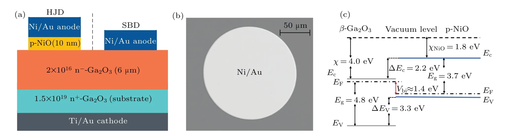
Fig.1.(a)Schematic cross-section of a vertical NiO/β-Ga2O3 HJD(left)and Ni/β-Ga2O3 SBD(right).(b)SEM anode surface image of an HJD.(c)Schematic energy band diagram of a NiO/β-Ga2O3 p–n heterojunction.
3.Results and discussion
The electrical properties of the devices are tested by a B1505A power device analyzer in the DC mode.The forward output curve of the HJD and SBD are shown in Fig.2(a),from which it can be seen that the turn-on voltage of the HJD and SBD are 1.85 V and 0.77 V respectively.Compared to conventional p–n junction diodes, HJDs possess certain performance advantages,including low turn-on voltages.By fitting the linear region of the output curve, it is calculated that the specific on-resistances of the HJD and SBD are 3.39 mΩ·cm2and 2.77 mΩ·cm2, which are far lower than that of the conventionalβ-Ga2O3SBD.[18]It can be seen from Fig.2(a)that the on/off current ratios of the HJD and SBD are as high as 108.As shown in Fig.2(b), theRon,spof the HJD increases~1.35 mΩ·cm2as the temperature (T) rises from 30°C to 140°C and then stabilizes at 4.75 mΩ·cm2.The Ga2O3HJD exhibitsT-independentRon,spbehavior similar to as in GaN p–n diodes.[19]Additionally,due to the bandgap narrowing effect and thermally-enhanced carrier diffusion,[5]the value ofVonreduces from 1.85 V to 1.55 V with elevated temperatures.And the value ofVonreduces from 0.77 V to 0.55 V.
The reverse breakdown characteristics of the HJD and SBD are shown in Fig.2(d).The breakdown voltages of the HJD and SBD are 465 V and 302.7 V respectively, and the Baliga’s FOM of the HJD is calculated to be 256 MW/cm2.The HJD presents optimal reverse current suppression capabilities when suffering from a reverse bias voltage of below 175 V to a reverse leakage current of less than 10-9A.Above 175 V, the HJD retains a leakage current of 10-8A, demonstrating its more remarkable reverse suppression capacity than the SBD.The leakage current of the HJD may be sustained at below 10-10A when the reverse voltage is less than 100 V,while the leakage current of the SBD is above 10-10A, and the HJD obtains a leakage current of 10-11A at a bias voltage of less than 60 V,which is shown in Fig.2(c).The HJDs present good reverse blocking performance.Compared with theβ-Ga2O3-based HJD fabricated by magnetron sputtering,the HJDs fabricated by thermal oxidation have superior stabilities and performance consistencies,laying a technological foundation for the preparation of high-performance Ga2O3-based devices.
To explore the temperature resistance characteristics of the device,the leakage current is tested under a 100 V reverse bias voltage.As shown in Fig.3(a), the device still maintains good reverse suppression performance at a temperature of 30°C–140°C.The reverse leakage current of the HJD is basically unchanged below 140°C,which is similar to that at room temperature.Figure 3(b)shows that the reverse leakage current of the HJD at 170°C is lower than one order of magnitude different from that at room temperature.Meanwhile,the reverse leakage current of the SBD increases at 140°C and 170°C,which is shown in Figs.3(a)and 3(b).Theβ-Ga2O3HJD shows good thermal stability and reliable performance at high temperatures.
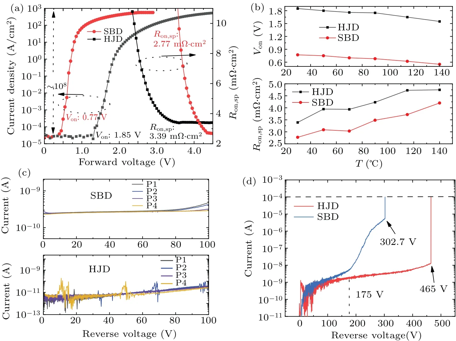
Fig.2.(a)The logarithmic curve of the forward characteristics of the HJD and SBD.(b)Forward temperature test curve of the HJD and SBD.(c)Test curve of HJDs and SBDs under 100 V reverse bias voltage.(d)The logarithmic curve of the reverse breakdown characteristics of the HJD and SBD.

Fig.3.(a)The test curve of the HJD and SBD under 100 V reverse bias and 30 °C–140 °C variable temperature.(b)The test curve of the HJD and SBD under 100 V reverse bias and 170 °C high temperature.(c)The logarithmic curve of the forward characteristics of the HJD and SBD.(d)ln(J)–V curve of the reverse characteristics of the HJD and SBD.
The four current transport processes of the device are analyzed.In the case of minimal current injection,the electron–hole complexation process in the space charge region dominates and exhibits complex current domination.And the current magnitude is proportional to exp(qVA/(2kBT)).When the current gradually increases to a certain degree,the device exhibits a low current injection process, in which the concentration of minority carriers injected into the drift region is much lower than the doping concentration in the drift region.The minority carrier diffusion process in the drift region dominates and exhibits a diffusion current,at which time the current magnitude is proportional to exp(qVA/(kBT)).When the concentration of injected minority carriers in the drift region exceeds the doping concentration in the drift region, the device reaches a high current injection process.The current transport depends on the high concentration of electrons and holes in the drift region, and the current magnitude is proportional to exp(qVA/(2kBT)).When the device’s forward current reaches a greater current density, the compounding effect in the end region reduces the carrier concentration injected into the drift region, which makes the forward voltage drop of the device increase and the device output current gradually tends to saturation.Cheung and Zhouet al.[20,21]have proposed that when the voltageVD=VA-JARS>3kBT/e(~0.08 V)is applied to the diode, the relationship between device voltageVAand current densityJcan be simplified as
Solving the differential equation ofVAabout lnJ,we can get
wheree,A,RS,n,kB,T,A*, and are the elementary charge,device area, series resistance, ideality factor, Boltzmann constant, temperature, effective Richardson constant, and Schottky barrier height at equilibrium(zero bias),respectively.The logarithmic curve of the HJD’s and SBD’s positive properties are shown in Fig.3(c).The HJD has a high rectifier ratio of 108.Under the positive output constraint, both the HJD and SBD reach an output current density of 560 A/cm2.The output current density of the HJD and SBD exceeds 100 A/cm2at 2.88 V and 1.15 V respectively.The ideality factor extracted from the fitting curve slope is 1.58(HJD) and 1.07(SBD).It can be concluded that the forward conduction current of the HJD is mainly compound current and diffusion current,while the forward conduction current of the SBD is mainly diffusion current.
The reverse leakage mechanism in Ga2O3-based vertical structure power diode devices is commonly explained using two methods:the thermionic-field emission(TFE)mechanism and variable range hopping conduction (VRH).According to the thermal electron field emission mechanism, formula (2)can be transposed and simplified as follows:
For variable range hopping, the leakage current is expressed as follows:[22]
with
where,C,E,Vbi, andWdare the constant, the electric field,the built-in potential,and the thickness of the drift region,respectively.The dependence ofJandEis ln(J)∝E, and the slope of the ln(J)–ln(E)fitting curve is close to 1.Figure 3(d)shows the ln(J)–Vcurve of the HJD and SBD after fitting the double logarithm curve.Through fitting analysis,the variable range jump conduction mechanism of the HJD can completely fit the whole leakage current curve,which clearly explains the mechanism of leakage current generation.Figure 4(a) shows the two-dimensional electric field distribution at a reverse bias of 500 V for the HJD,using Silvaco TCAD software.Electric field profiles along the cutline at the device edge have been extracted and are shown in Fig.4(b).The peak electric field of the HJD reaches the value of 7.9 MV/cm.The magnitude of the peak electric field for the HJD device has almost reached the theoretical Ga2O3breakdown electric field(8 MV/cm).
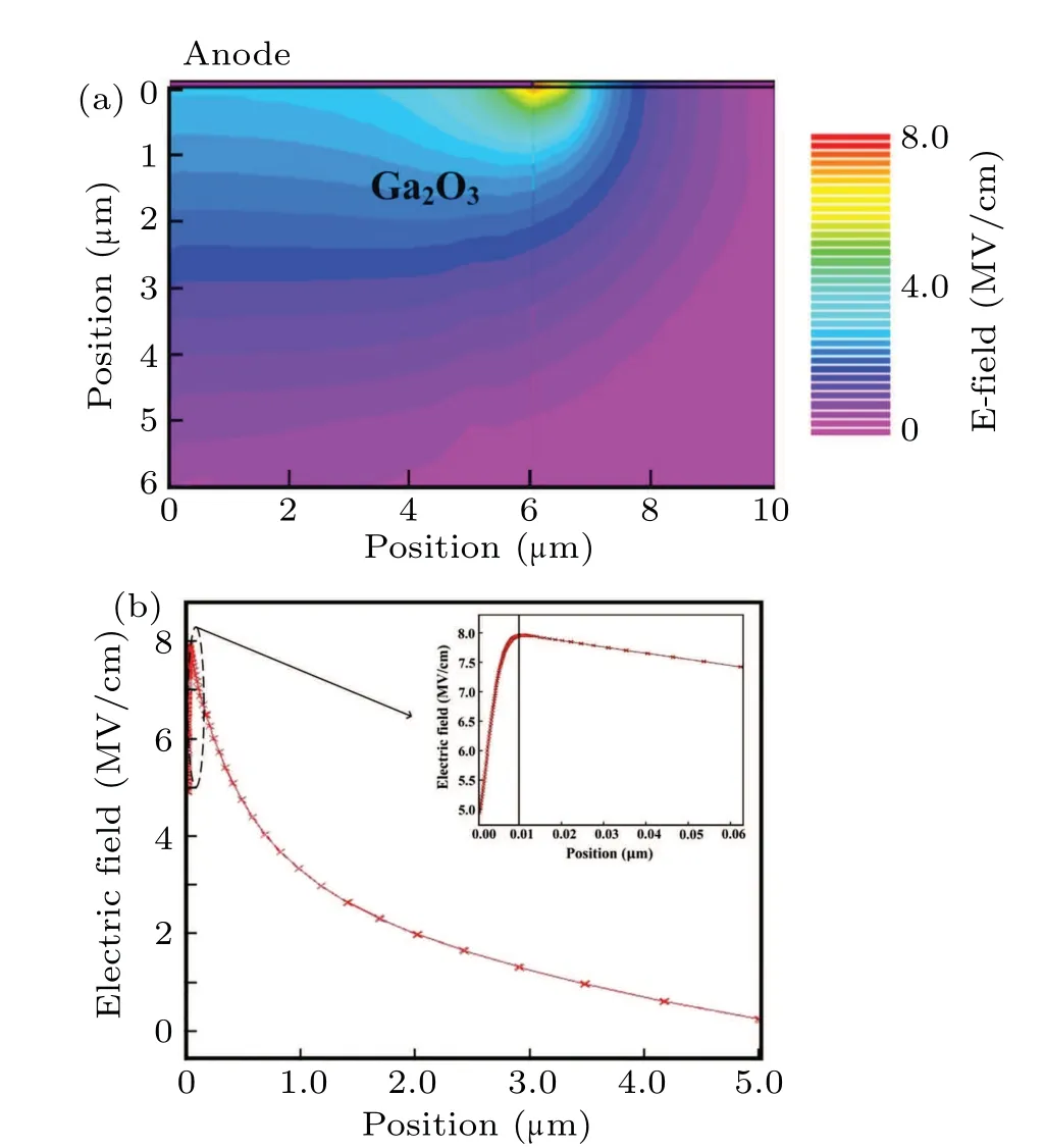
Fig.4.(a)Two-dimensional electric field distributions at a reverse bias of 500 V of the HJD device simulated by Silvaco TCAD software.(b)Extracted electric field profiles along the cutline at the device edges of the HJD device.
4.Conclusion
In summary,β-Ga2O3HJDs with p-NiO prepared by thermal oxidation processes are studied.The high breakdown voltage(465 V),turn-on voltage(1.85 V),and low specific onresistance(3.39 mΩ·cm2)of the HJD are obtained.The HJD structure efficiently reduces conduction loss and improves electrical performance.Moreover,the performance of the HJD is equivalent to that of an HJD formed by magnetron sputtering.The reverse leakage current of NiO/β-Ga2O3HJDs can always remain around 10-10A when the temperature varies from 30°C to 140°C, indicating that Ga2O3HJDs have great practical potential for high-temperature,high-power,and high-reliability applications.
Acknowledgements
Project supported by the Technology Innovation and Application Demonstration Key Project of Chongqing Municipality (cstc2019jszx-zdztzxX0005), the Technology Innovation and Application Demonstration Key Project of Chongqing Municipality (cstc2020jscx-gksbX0011), the Science and Technology Research Program of Chongqing Municipal Education Commission(KJQN202100614),and the Natural Science Foundation of Chongqing(cstc2021jcyj-bshX0146).

- Chinese Physics B的其它文章
- Robustness of community networks against cascading failures with heterogeneous redistribution strategies
- Identifying multiple influential spreaders in complex networks based on spectral graph theory
- Self-similarity of complex networks under centrality-based node removal strategy
- Percolation transitions in edge-coupled interdependent networks with directed dependency links
- Important edge identification in complex networks based on local and global features
- Free running period affected by network structures of suprachiasmatic nucleus neurons exposed to constant light