多次透射反射紅外光譜法靈敏和準確地測量單晶硅中間隙氧和代位碳的含量
2016-11-28 09:36:38路小彬肖守軍
無機化學學報 2016年2期
路小彬 肖守軍
(配位化學國家重點實驗室,南京大學化學化工學院,南京210093)
多次透射反射紅外光譜法靈敏和準確地測量單晶硅中間隙氧和代位碳的含量
路小彬肖守軍*
(配位化學國家重點實驗室,南京大學化學化工學院,南京210093)
建立了室溫下使用多次透射反射紅外光譜法(MTR-IR)測量單晶硅中間隙氧和代位碳含量的新紅外光譜吸收方法,在理論和實驗上證明了MTR-IR優于常規使用的單次垂直透射紅外(IR)吸收測量方法。與IR法相比較,MTR-IR法的優點為:(1)間隙氧在1 107 cm-1處和代位碳在605 cm-1處的吸收峰與MTR-IR法中紅外光透過硅片的的次數N(6~12)成線性增加的正比例關系,因此單晶硅中間隙氧和代位碳含量的檢測限至少比IR法低一個數量級;(2)MTR-IR法測量薄硅片如0.2 mm的厚度時產生的干涉條紋強度是單次垂直透射紅外吸收法(IR)的1/23、是單次Brewster角透射紅外吸收法的1/11;(3)單次垂直透射紅外吸收法(IR)1次只測量樣品上的1個點,MTR-IR法則在更長的樣品上1次測量多個樣品點,每次測量更具有代表性。理論計算和實驗結果都證實了MTR-IR吸收法測量晶體硅中間隙氧和代位碳雜質含量的高靈敏度、可靠性和重復性。
多次透射反射;紅外;間隙氧;代位碳
0Introduction
Silicon-basedsemiconductorindustry,asa miracle in the human beings history,continues to develop at considerably high growth rates already for half a century.Recently,solar energy has been recognized in common as an alternative sustainable energy source due to the increased awareness of the global energy crisis[1].Silicon solar cells have become the most important photovoltaic products owing to the sophisticatedmanufacturingtechnologyandthe reliable cell quality.The quality control of silicon materials is crucial to both semiconductor and solar cell industries of silicon.During the Czochralski(CZ) procedureingrowingsiliconsinglecrystalsfor semiconductor and photovoltaic industry,oxygen and carbon are incorporated into the molten silicon to different extents from the quartz crucibles and the graphite heaters.As oxygen atoms can find sites within the lattice structure among silicon atoms, interstitial oxygen(Oi)appears.Moreover,carbon atoms occupy positions generally taken by silicon atoms in the lattice structure,and this kind of impurity is defined as substitutional carbon(Cs)[1-3].
Interstitial oxygen and substitutional carbon are the main forms of oxygen and carbon impurities existinginsilicon.Theirdifferentlevelscause different physical and electrical effects in silicon, whichhavebeenextensivelyinvestigatedand correlated[4-6].Although Oi in suitable concentrations possesses an advantage to enhance the mechanical strength of silicon because of its nailing for stretching ofdislocationinthesiliconlattice,higher concentrations will result in electrically active defects that decrease the performance of the devices.Thus a gettering technique has been developed to decrease Oi and avoid defects during the silicon crystal growth procedure.High content of Cs affects the way Oi nucleates and precipitates,as well as resulting in softening and breakdown of electronic components[7-10]. Consequently,to control the silicon quality for high performance devices,it is absolutely necessary to monitor the content of Oi and Cs in silicon wafers more accurately and sensitively.
Varioustechniqueshavebeenappliedto determine the content of Oi and Cs in bulk silicon. Thesetechniquesconsistofgasfusionanalysis, secondary ion mass spectrometry,charged particle activation analysis and neutron activation analysis etc.,all of which are destructive,costly and time consuming[1].In addition,the above methods measure the total content of elemental oxygen and carbon, including Oi and Cs and other forms of oxygen and carbon.Thus they are not specific for measuring the concentration of Oi(atoms per cm3,abbreviated as cOi, cm-3)and of Cs(atoms per cm3,abbreviated as cCs, cm-3).By contrast,infrared analysis is specific to cOiand cCsin silicon.Silicon atoms form bonds with the adjacent oxygen atoms(Si-O-Si)and carbon atoms(Si-C)in the lattice structure[11-13].The interstitial oxygen is in the form of Si-O-Si,giving three vibration peaks centered at 1 107 cm-1(strong),513 cm-1(medium) and 1 718 cm-1(weak)respectively.Among the three bands,the strongest one at 1 107 cm-1is usually used to determine cOi[14-16].The substitutional carbon in the form of Si-C gives a vibration band at 605 cm-1. However the Si-C band overlaps with the strong silicon lattice vibration(Si-Si)at 605 cm-1,which renders the measurement of cCsdelicate.The amount of light absorbed by Si-O-Si and Si-C is proportional to the concentration of atoms forming the bonds.Thus their corresponding infrared bands are measured and manipulated to quantitate cOiand cCsrespectively.The calculation procedure is composed of subtraction of a reference(free of Oi and Cs)absorption band from a samples band,and subsequently calculation of cOiand cCsusing the following formulae generally.
A=αbα=εc
where A is the measured absorbance;ε is the absorption coefficient of a particular bond,cm2;b is the thickness of the sample,cm;c is the concentration of the impurity,cm-3.
The IR method for the levels of Oi and Cs can be carried out at ambient or low temperature.Although the latter is more accurate than the former,it is costly and time consuming to handle the measurement at thecryogenic temperature.Furthermore,the reflection loss of infrared light at both cryostat windows outweighs its advantages[17-20].
The room temperature IR method for cOiand cCsmeasurements is most commonly used in industry because it is easy and simple to operate.Generally the presentlyacceptedstandardmethodusedin industry for cOiand cCsmeasurements is restricted to a silicon slice with a thickness of 2 mm and a diameter of the infrared beam by a one-time perpendicular transmission of the infrared beam(we name it“conventional IR”).The detection limits of cOiand cCsfor a 2.0 mm thick single crystalline silicon are 1×10¹⁶and 5×1015cm-3respectively[21-22].The above quantitative analysis meets challenges in practice such as:1) measurement errors become larger when cOiand cCsreachtheirowndetectionlimits,2)interference fringes from thin wafers below 0.3 mm thickness interferethetargetbandsignal,3)thesingle transmission measurement approach in a spot provides a localized spectrum with poor specimen statistics, compared to the multi-spot data collection in MTR-IR. Our newly developed MTR-IR(Scheme 1)provides an excellent quantitative approach for analysis of cOiand cCs,duetoitsuptooneorderofmagnitude enhancement of infrared absorption signals on the samesiliconslicefromtheconventionalIR measurement[23-26].In this letter,we applied the MTRIR spectroscopy in analysis of cOiand cCsof 0.45 mm thick silicon wafers.Our MTR-IR method greatly improves the measurement sensitivity and accuracy, for example,reaching detection limits of cOiat 1×1015cm-3and cCsat 5×1014cm-3for the standard silicon specimens with a 2.0 mm thickness,which is one order of a magnitude lower than from the standard method.MTR-IRalsoattenuatestheinterference fringes of thin wafers greatly,and advances the representativeness of data collections.
Scheme 1Scheme of the MTR-IR optical path
1 Experimental
1.1Substrates
Double-side-polished and〈100〉oriented n-type silicon wafers(B doped,resistivity of 15 Ω·cm(CZ) and 3 000 Ω·cm(FZ)respectively,0.45 mm thick, from Shanghai Junhe Electronic Materials Co.Ltd., China)were cut into rectangular shapes(16 mm×50 mm)for infrared analysis.CZ silicon wafers were used as samples and FZ as reference to measure the impurity concentrations of Oi and Cs respectively.
1.2Wafer cleaning
Siliconwaferswerecleanedwith“piranha solution”(concentrated H2SO4/30%H2O2,3∶1,V/V)for 4 h(caution:piranha solution reacts violently with organic materials and should be handled with great care)to remove organic pollutants,followed by boiling in the mixture of NH3·H2O/H2O/H2O2(1∶1∶1,V∶V∶V) for 30 min,then cooling to room temperature,rinsing with water,and storing in water.Silicon samples were immersed in 1%HF for 5 min to eliminate the native passivation silicon oxide layer,and dried with a stream of nitrogen just before the measurement.
1.3Measurement
The optical setup was designed to adapt to any commercial FTIR spectrometers,which is Bruker 80v FTIR,in our case.MTR accessory with a Brewster incident angle of 74°was used.Unless specified,a DTGS detector and scan times of 100 at 4 cm-1resolutionwereusedformeasurementoverthewavenumber range from 400 to 4 000 cm-1.
The silicon sample was inserted between the two Aumirrors,withoneendofthesiliconslice protruding about 5 mm out of the incident spot,in order to make sure that the first incidence shot was on the silicon surface.The two guiding mirrors can be moved back and forth to get the maximal luminous flux in the DTGS detector.The incident angle was controlled at 74°by a micro-adjuster with a minimal angle scale of 0.225.
The whole measurement procedure was performed according to ASTM F 1188 and ASTM F 1391[21-22,30]. Eight random samples from different batches were used.Each sample was measured successively 4 times by MTR and IR by slightly relocating the Si wafer each time in order to measure different sampling points.Therefore for each sample,4 different sampling points were measured by IR,whereas 40 different sampling points measured by MTR-IR if N equals 10. 1.4Theory/calculation
1.4.1Comparisonofcomputationmodelsfor
conventional IR and MTR-IR
1.4.1.1Conventional IR method
In the conventional IR method,the normal incident light passes a Si wafer(for convenience,a slightly oblique incidence is drawn in Fig.1),the transmittance canbeexpressedasinEq.(1)and(2)[21-22].
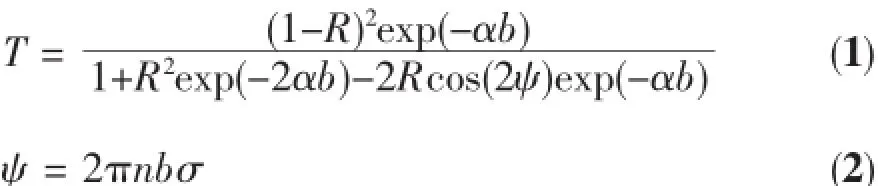
where T is the transmittance of normal incidence, %;R is reflectivity;n is refractive index;σ is wavenumber,cm-1;ψ is the phase change due to the interfering multiple reflections on the boundaries of the sample.
1.4.1.2Brewster angle single incidence
The expression of TBfor the single Brewster incidence refers to Eq.(3)[29].
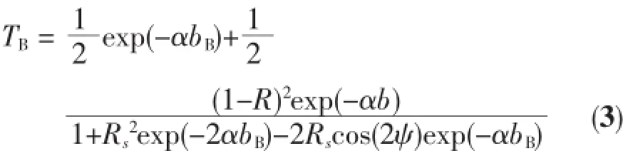
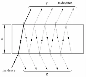
Fig.1 Light path of computation model for IR
where TBis the transmittance of the Brewster angle single transmission,%;Rsand Rpindicate the reflectance of s-and p-polarization respectively;the first(Rp=0)and the second term(Rshas a value)in the formula represent transmittance energy of ppolarization and s-polarization respectively,because the total transmittance energy equals the sum of ppolarization and s-polarization(p-or s-polarization holds 1/2 of the original light energy);the phase change introduced by the interfering multiple reflections on the boundaries of a silicon is considered.
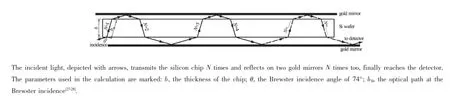
1.4.1.3MTR method[27]
The light path of the computation model for MTR-IR refers to Scheme 1.Comparing Scheme 1 to Fig.2,we observed that two gold mirrors enforce the light transmit through the silicon slice N times and simultaneously taking away the message of oxygen and carbon of the silicon sample.The optical path in the MTR-IR setup of Scheme 1 is N times of bBat theBrewster incidence.For simplicity,only the main light path is drawn in Scheme 1 with N=6,all other light paths by multiple reflections in the MTR setup are ignored.The transmittance for MTR-IR(TMTR)is deduced as follows(See supporting information for details of derivation of the formula of MTR-IR):
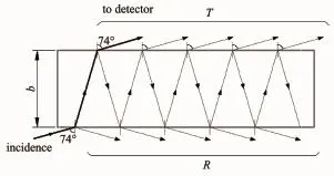
Fig.2 Light path of the computation model for Brewster angle single transmission
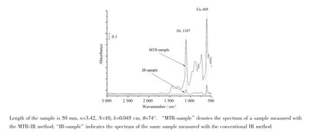
Fig.3 Comparison of Oi and Cs spectra for MTR-IR and conventional IR
where TMTRis the transmittance of MTR,%;RAuis the reflectivity of gold;bMTRis the optical path through a silicon sample in the MTR-IR measurement,cm. 1.4.2Theory of signal enhancement of MTR-IR
Presently,theconventionalIRmethodfor measurement of cOiand cCsis to place a 2 mm thick single crystalline silicon slice normally(or within the margin of error of a slightly oblique angle≤10°)in the light path.The sampling length equals to the thickness of the slice.The illuminated area is a circle with a diameter of the light spot,so the resulting cOiand cCsjust represent the impurities within a cylinder with a diameter of the light spot(depending on the aperture)and a height of 2 mm.Whereas in the MTRIR setup,the infrared light reflects back and forth manytimesbetweentwogoldmirrorsand simultaneously passes through the sampling silicon slice repeatedly and takes away the information of Oi and Cs by the resonance of Si-O-Si and Si-C bonds. So,the optical path is N(1+1/n2)1/2times of the thickness of a silicon wafer(b),and correspondingly the absorbance is amplified N(1+1/n2)1/2times[29].
At the Brewster angle of 74,when Rp=0,Rs=0.70, RAu=1,the phase change of p polarization light ψ=π, the following formula can be deduced from Eq.(1)and(4).
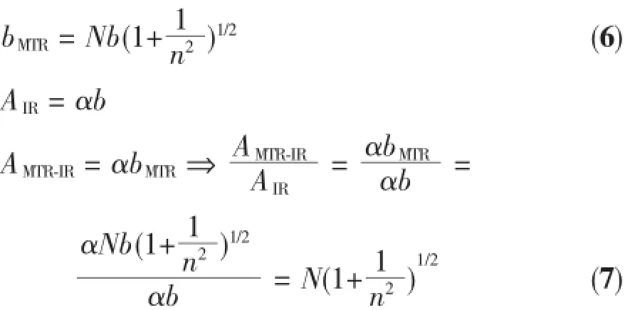
From Eq.(6),the sampling length is enlarged N(1+1/n2)1/2times,assuming the recorded infrared spectral signal comes from the main optical path illustrated in Scheme 1,and all other infrared signals are ignored.The infrared light passes through a silicon slice N times in different regions,thus the collected signal is an integrated one of the whole optical path,physically and statistically representing Oi and Cs in the silicon slice better.
2 Results and discussion
2.1Comparison of infrared traces between the conventional IR method and the MTR-IR method
We listed two spectral traces of the same sample in Fig.3,where the upper trace was obtained from MTR-IR and the lower trace from the conventional IR. All bands bear the same shape but their absorbance strength in MTR-IR is much higher than from IR, especially for the two strongest bands of Oi at 1 107 cm-1and Cs at 605 cm-1.From the view point of quantitation,the bigger the absorbance value,the less the measurement error of Oi and Cs.Consequently cOiand cCsare more accurate and will have a lower detection limit.Because the absorption of Cs at 605 cm-1overlaps with the strongest absorption of the silicon lattice vibration(Si-Si)centered at 610 cm-1,a FZ silicon reference is needed to subtract the silicon lattice vibration.Further,the real advantage of MTRIR over the conventional IR not only lies in its ability to measure the spectra of Oi and Cs with stronger signals,but also with more sampling points for robust and representative measurements.
In Fig.3,the peak height ratios of Oi and Cs (MTR-sample/IR-sample)were measured to be~10 and~8 respectively.Generally speaking,cCsis more difficult to be measured than cOiusing the conventional IR method,due to two factors:(1)It is very tough to extract the much smaller Si-C peak from the strong Si-Si lattice band and therefore artificial results are often derived individually,thus an accurate quantitation is nearlyimpossible.(2)TheCslevelinsingle crystalline silicon is always an order of magnitude lowerthanthatofOi.Judgedfromthesignal enhancement,it is possible to extend the limit of detection of cOiat 1×10¹⁶to 1×1015cm-3and cCsat 5× 10¹⁵to 5×1014cm-3for a 2.0 mm thick single crystalline silicon.
We randomly chose 8 samples to measure their cOiand cCs,both by the conventional IR and the MTRIR methods,for verification of the MTR-IR method by the correlation curve in Fig.4a and 4b(calculation details please see Supporting Information:2.Data calculation).As it can be seen in Fig.4a and 4b,both cOiandcCsarelinearlycorrelated.Thelinear relationshipofbothcOiandcCsprovedthe measurement accuracy of the MTR-IR method for determination of cOiand cCsin single crystalline silicon materials.
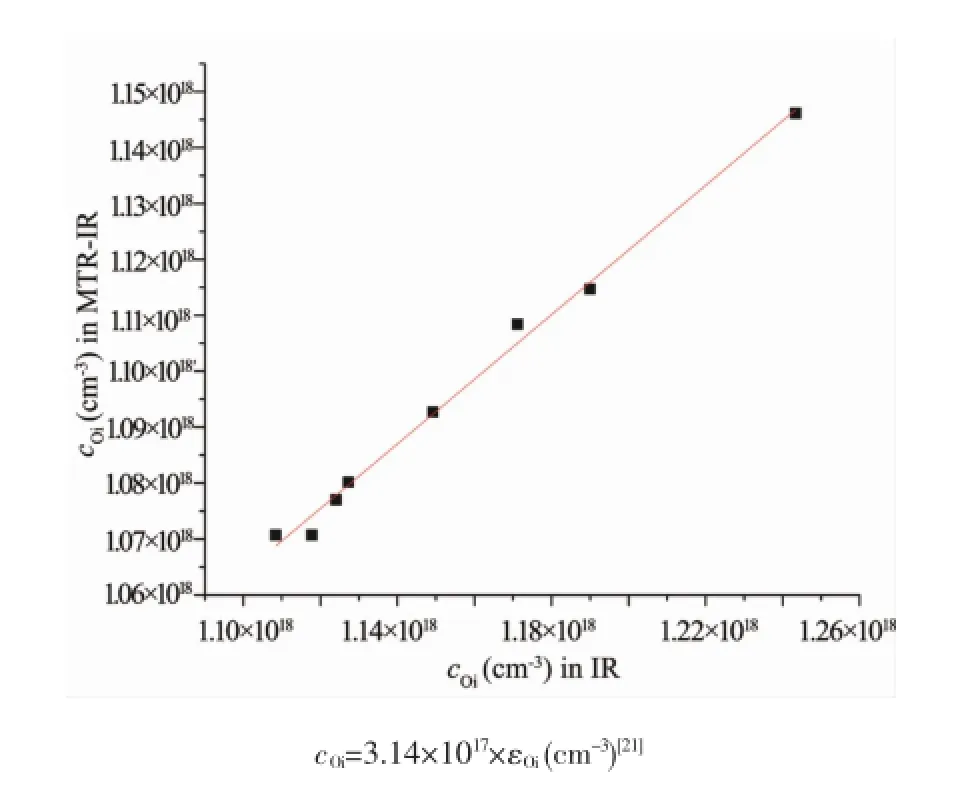
Fig.4 aOi concentration at 1 107 cm-1for eight samples measuredbyMTR-IRvsconventionalIR
The interference fringes become much stronger when a silicon wafer thickness is close to the infrared wavelength.Thefringesarewellrecognizedto interrupt the IR measurement,they obscure the weak features of the spectra,as well as reduce the accuracyof quantitative analysis.Both IR and MTR-IR are able to measure a silicon slice with a thickness above 0.3 mmbecausethemultiplebeamsresultedfrom multiple reflections and transmissions are out of phase andthusthesebeamsgenerateneglectable interference fringes[29].
However,when the sample thickness is less than 0.2 mm,the interference fringes become more obvious and cannot be ignored when measuring Oi and Cs. The amplitude of interference fringes depends on the interaction mode between the incident light and the sample.Eq.(1),(3)and(4)are used to calculate the transmittance of three modes respectively:normal incidence,Brewster angle single transmission,and MTR.For the Brewster angle incidence,RPis equal to 0,while RSis 0.70.Obviously the oscillation of transmittance is derived from the phase change of ψ, thus the p-polarization does not cause any oscillation of transmittance at the Brewster angle incidence.In (1),the whole term affects the amplitude of oscillation, while in(3)and(4),the second term bearing the phase change of ψ becomes weaker and weaker when N increases.Therefore the amplitude of oscillations must be reduced with increasing N.In Fig.5,the variation of oscillations caused by phase change(ψ)is shown for the normal incidence,the Brewster angle single transmission,and the MTR mode respectively. The amplitude of the oscillationis 0.058for the normal incidence(T),0.029 for the Brewster angle single transmission(TB),and only 0.002 5 for the MTR-IR approach(TMTR).In this case,theoretically compared to the normal incidence,the Brewster angle single transmission reduces the oscillation amplitude by a factor of 2,whereas,the MTR setup reduces the oscillation amplitude by a factor of 23.The above theoretical analysis demonstrates the overwhelming advantages of the MTR setup for measuring cOiand cCsin a thin silicon slice.
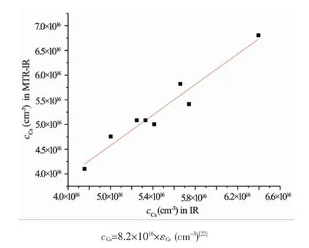
Fig.4bCs concentration at 605 cm-1for eight samples measured by MTR-IR vs conventional IR
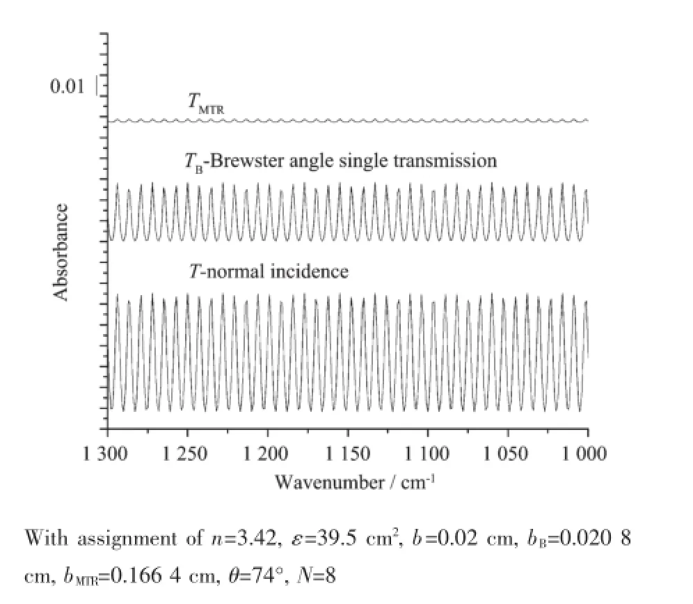
Fig.5Theoretical simulation of the transmittance oscillations as a function of the wavenumber σ calculated from Eq.(1),(3)and(4), corresponding to the normal incidence, the Brewster angle single transmission and MTR respectively
To prove the theoretical calculation,we recorded the spectra of a 0.20 mm thin silicon wafer in Fig.6with normal incidence(bottom trace as“normal incidence”),Brewsteranglesingletransmission (middle trace as“Brewster angle single transmission”) and MTR(upper trace as“MTR”)respectively.From the three curves,it is easily observed that interference fringes appear heavily for the normal incidence, moderately for the Brewster angle single transmission, and negligibly for the MTR.The interference fringe strengthratiosofMTR/Brewsteranglesingle transmission/normal incidence are close to 20∶2∶1 in most regions.
From Fig.6,not only the interference fringes in MTR-IR are greatly attenuated,the target signals inthe region of 400 to 1 200 cm-1are also significantly magnified.Thus the signal to noise ratio is enhanced several orders of magnitude higher in MTR for much thinner silicon slices less than 0.3 mm thickness.The use of a thin silicon wafer can decrease the sampling volume,save the cost of an experiment,and fits the requirements of the solar energy industry.From both thetheoreticalcalculationsofFig.5andthe experimental spectra of Fig.6,obviously the currently used standard IR method is not suitable,whereas MTR-IR is much more powerful for measurement of Oi and Cs in a thin silicon slice less than 0.3 mm thick.That is also why MTR-IR is needed urgently for the silicon solar cell industry.
Finally,we present the evolution of 7 infrared traces against N in Fig.7a.We have demonstrated the linear relationship of the absorbance strength of a band against the number of simplified transmission times(N) in our previous report[23].Since the detection limit of an analysis method depends on the signal to noise ratio. For the measurements of Fig.3 and Fig.7a,their baselines are flat enough,therefore,we can assign the spectral noise from 0.3~2.0 mm thick silicon samples to the instrumental noise,which possess the same value. With this hypothesis,we can deduce the detection limits of Oi and Cs,shown in Fig.7b,at different N from 6 to 12 by dividing the standard detection limits with the peak magnification times of MTR/normal incidence (peak height of Oi or Cs in Fig.7/peak height of Oi or Cs in IR-sample in Fig.3).It is observed that our MTRIR method significantly improves the detection limits of cOiand cCsfor the standard 2.0 mm thick single crystalline silicon,reaching cOiand cCsat 1×10¹⁵and 5× 1014cm-3,respectively.
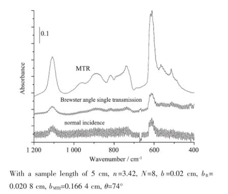
Fig.6Experimental results of interference fringes corresponding to normal incidence,Brewster angle single transmission and MTR respectively
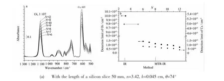
Fig.7(a)Variation of the absorbance of Oi and Cs in silicon wafers vs N from the MTR setup(b)Comparison of the limit of detection of cOiand cCsin silicon wafers measured with IR and MTR-IR
3 Conclusions
In conclusion,our experiments confirm that the MTR-IR method can reach a higher sensitivity and better spectral quality than the most commonly used conventional IR.The signal of the Oi peak at 1 107 cm-1obtained by MTR can be enhanced 10 times than by the conventional IR method,the one of the Cs peak at 605 cm-18 times.The MTR sampling length is N(1+1/n2)1/2times long as the one in the conventional IR,thus the measured cOiand cCsare morerepresentative.SinceMTR-IRreducestheinterference fringes greatly for silicon slices with a thickness thinner than 0.3 mm,it will be the most powerful tool to characterize the ultrathin silicon wafers and therefore the portable and foldable silicon devices.Due to its simple operation,MTR-IR satisfies thepracticalneedsinindustrialapplications, especially for semiconductor and silicon solar cell industries.
Several parameters still need improvement in further works.For example,the theoretical equations are deduced from the main light path,neglecting other multiple reflections and transmissions on silicon and gold mirrors.The MTR formulas still need more experimental data for calibration.
Considering the conclusion above,we believe that the MTR-IR method will be established as a standard method for measurement of interstitial oxygen andsubstitutionalcarbonforcrystallinesilicon materials.
Acknowledgments:We acknowledge financial support from the National Basic Research Program of China(No. 2013CB922101)and the NSFC,No.91027019.
Supporting information is available at http://www.wjhxxb.cn
References:
[1]Boyle R.Thermo Scientific Application Note,2008,50640:1-4
[2]CravenRA,KorbHW.SolidStateTechnol.,1981,24(7):55-61
[3]Benson K E,Lin W,Martin E P.Semiconductor Silicon 1981.Pennington N.J.:Electrochem.Soc.Inc.,1981:33-48
[4]Abe T,Kikuchi K,Shirai S,et al.Semiconductor Silicon 1981.Pennington N.J.:Electrochem.Soc.Inc.,1981:54-71
[5]Rava P,Gatos H C,Lagowski J.Semiconductor Silicon 1981.PenningtonN.J.:Electrochem.Soc.Inc.,1981:232-243
[6]Ohsawa A,Honda K,Yoshikawa M.Fujitsu Scie.Techn.J., 1980,16(3):123-134
[7]Kishino S,Matsushita Y,Kanamori M.Appl.Phys.Lett., 1979,35(3):213-215
[8]Ogino M.Appl.Phys.Lett.,1982,41(9):847-849
[9]Oehrlein G S,Lindstrom J L,Corbett J W.Appl.Phys.Lett., 1982,40(3):241-243
[10]Ohsawa A,Takizawa R,Honda K,et al.Appl.Phys.,1982, 53(8):5733-5737
[11]Pajot B.Analusis.,1977,5:293-303
[12]Hrostowski H J A B J.J.Chem.Phys.,1960,33:980-990
[13]Corbett J W,Mcdonald R S,Watkins G D.J.Phys.Chem. Solids,1964,25:873-879
[14]Kaiser W,Keck P H,Lange C F.Phys.Rev.,1956,101(4): 1264-1267
[15]Kaiser W,Keck P H.J.Appl.Phys.,1957,28(8):882-885
[16]Kaiser W,Frisch H L,Reiss H.Phys.Rev.,1958,112(5): 1546-1554
[17]Bosomworth D R,Hayes W,Spray A R L,et al.Royal Soc. London,1970,317(1528):133-152
[18]Pajot B,Deltour J P.Infrared Phys.,1967,7:195-200
[19]Oeder R,Wagner P.Defects in SemiconductorsⅡ.N.Y.: North-Holland,1983:171-175
[20]Kolbesen B O,Kladenovi T.Krist.Tech.,1980,15(1):k1-k3
[21]ASTM.Designation F1188:Test Method for Interstitial Atomic Oxygen Content of Silicon by Infrared Absorption.
[22]ASTM.Designation F1391:Test Method for Substitutional Atomic Carbon Content by Infrared Absorption.
[23]Liu H,Xiao S,Chen Y,et al.J.Phys.Chem.B,2006,110 (36):17702-17705
[24]Guo P,Liu H,Liu X,et al.J.Phys.Chem.C,2010,114(1): 333-341
[25]Liu H,Venkataraman N V,Bauert T E,et al.J.Phys.Chem. A,2008,112(48):12372-12377
[26]LiuH,VenkataramanNV,SpencerND,etal.Chemphyschem, 2008,9(14):1979-1981
[27]LIU Hong-Bo(劉洪波).Thesis for the Doctorate of Nanjing University(南京大學博士論文).2008.
[28]Xiao S,Liu H,Tobias B.China Patent,2006,10097859.4. 2006-11-16.
[29]Leroueille J.Appl.Spectrosc.,1982,36(2):153-155
[30]Baghdadi A,BullisWM,CroarkinMC,etal.J. Electrochem.Soc.,1989,136(7):2015-2024
Sensitive and Accurate Measurement of Interstitial Oxygen and Substitutional Carbon in Single Crystalline Silicon by Multiple Transmission-Reflection Infrared Spectroscopy(MTR-IR)
LU Xiao-BinXIAO Shou-Jun*
(State Key Laboratory of Coordination Chemistry,School of Chemistry and Chemical Engineering,Nanjing University, Nanjing 210093,China)
A new infrared spectroscopic measurement of interstitial oxygen and substitutional carbon in silicon wafers at room temperature by Multiple Transmission-Reflection Infrared Spectroscopy(MTR-IR)has been established.The superiority of MTR-IR to conventional IR has been analyzed first in principle by theoretical calculation and then verified by practical measurements of single crystalline silicon samples.The advantages of MTR-IR over conventional IR with a single normal incidence are:(1)The absorption bands of interstitial oxygen at 1 107 cm-1and substitutional carbon at 605 cm-1can be enhanced linearly with the simplified transmission times(N)between 6 and 12,which consequentlyextendsthe detection limit of oxygen and carbon at least one order of magnitude lower.(2)The strength of interference fringes can be decreased for a 0.2 mm thin silicon slice by 23 times as that from the single normal incidence and 11 times as that from the Brewster angle transmission respectively.(3)Not like the conventional IR method,only collecting data from one sampling point at each measurement,MTR-IR collects data from multiple sampling points in a longer sample for one measurement.Overall,both theoretical calculations and experimental results demonstrate the high sensitivity,reliability,and reproducibility of the MTR-IR spectroscopy on the measurement ofimpurities of interstitial oxygen and substitutional carbon of single crystalline silicon.
multiple transmission-reflection(MTR);infrared Spectroscopy(IR);interstitial oxygen;substitutional carbon
O611.5
A
1001-4861(2016)02-0351-09
10.11862/CJIC.2016.044
2015-11-03。收修改稿日期:2015-12-03。
國家重點基礎研究發展計劃(No.2013CB922101),國家自然科學基金(No.91027019)資助項目。
*通信聯系人。E-mail:sjxiao@nju.edu.cn
猜你喜歡
中學生數理化·八年級物理人教版(2019年9期)2019-11-25 07:33:02
中學生數理化·八年級物理人教版(2019年3期)2019-04-25 06:20:54
中學生數理化·八年級物理人教版(2018年3期)2018-05-31 08:52:45
數學小靈通(1-2年級)(2017年10期)2017-11-08 08:39:45
科技知識動漫(2017年7期)2017-08-09 19:52:45
科技知識動漫(2017年5期)2017-05-11 21:34:16
科技知識動漫(2017年4期)2017-04-15 22:24:55
科技知識動漫(2017年2期)2017-02-06 20:59:46
科技知識動漫(2016年10期)2016-10-18 20:35:00
少兒科學周刊·兒童版(2016年1期)2016-03-14 03:52:21