Direct measurement and analysis of total ionizing dose effect on 130 nm PD SOI SRAM cell static noise margin?
2017-08-30 08:26:10QiwenZheng鄭齊文JiangweiCui崔江維MengxinLiu劉夢新DandanSu蘇丹丹HangZhou周航TengMa馬騰XuefengYu余學峰WuLu陸嫵QiGuo郭旗andFazhanZhao趙發(fā)展
Chinese Physics B 2017年9期
關鍵詞:發(fā)展
Qiwen Zheng(鄭齊文),Jiangwei Cui(崔江維),Mengxin Liu(劉夢新),Dandan Su(蘇丹丹),3, Hang Zhou(周航),3,Teng Ma(馬騰),3,Xuefeng Yu(余學峰),Wu Lu(陸嫵), Qi Guo(郭旗),and Fazhan Zhao(趙發(fā)展),?
1 Key Laboratory of Functional Materials and Devices for Special Environments,Xinjiang Technical Institute of Physics and Chemistry, Chinese Academy of Sciences,Urumqi 830011,China
2 Xinjiang Key Laboratory of Electronic Information Material and Device,Urumqi 830011,China
3 University of Chinese Academy of Sciences,Beijing 100049,China
4 Key Laboratory of Silicon Device Technology,Chinese Academy of Sciences,Beijing 100049,China
Direct measurement and analysis of total ionizing dose effect on 130 nm PD SOI SRAM cell static noise margin?
Qiwen Zheng(鄭齊文)1,2,Jiangwei Cui(崔江維)1,2,Mengxin Liu(劉夢新)4,Dandan Su(蘇丹丹)1,2,3, Hang Zhou(周航)1,2,3,Teng Ma(馬騰)1,2,3,Xuefeng Yu(余學峰)1,2,Wu Lu(陸嫵)1,2, Qi Guo(郭旗)1,2,and Fazhan Zhao(趙發(fā)展)4,?
1 Key Laboratory of Functional Materials and Devices for Special Environments,Xinjiang Technical Institute of Physics and Chemistry, Chinese Academy of Sciences,Urumqi 830011,China
2 Xinjiang Key Laboratory of Electronic Information Material and Device,Urumqi 830011,China
3 University of Chinese Academy of Sciences,Beijing 100049,China
4 Key Laboratory of Silicon Device Technology,Chinese Academy of Sciences,Beijing 100049,China
In this work,the total ionizing dose(TID)effect on 130 nm partially depleted(PD)silicon-on-insulator(SOI)static random access memory(SRAM)cell stability is measured.The SRAM cell test structure allowing direct measurement of the static noise margin(SNM)is specifically designed and irradiated by gamma-ray.Both data sides’SNM of 130 nm PD SOI SRAM cell are decreased by TID,which is different from the conclusion obtained in old generation devices that one data side’s SNM is decreased and the other data side’s SNM is increased.Moreover,measurement of SNM under different supply voltages(Vdd)reveals that SNM is more sensitive to TID under lower Vdd.The impact of TID on SNM under data retention Vddshould be tested,because Vddof SRAM cell under data retention mode is lower than normal Vdd. The mechanism under the above results is analyzed by measurement of I–V characteristics of SRAM cell transistors.
silicon-on-insulator,total ionizing dose,static random access memory,static noise margin
1.Introduction
The stability of the cell is very important for static random access memory(SRAM)cell design,determining the soft-error rate and the sensitivity of memory to process tolerances and operating conditions.[1]The static noise margin (SNM)of a cell is a measure of its stability.It can be extracted by nesting the largest possible square in the two voltage transfer curves(VTC)of the involved complementary metal-oxide semiconductor(CMOS)inverters,as shown in Fig.1.The total ionizing dose(TID)effect can affect the stability of the SRAMcell,because it primarily increases leakage and induces threshold shift in the transistor and SNM is determined by electrical characteristics of SRAM cell transistors.[2]Therefore,the stability of SRAM cell used in space should depend on TID that it receives in space.
The impact of TID on the stability of SRAM cell has been investigated for several decades.[3–13]TID will result in a preferred state and non-preferred state in SRAM cell.That is, SNM of data applied on cell during TID exposure is increased, whereas SNM of TID complement data is decreased.In general,SNM of SRAM before and after TID irradiation is determined by circuit simulation with the irradiated transistor model.[6,9–13]Simulation results are experimentally verified by single event upset(SEU)characterization[3,5–8]or background data[4,11]testing indirectly,according to the relationship between SNM and SEU cross section,and background data distribution.TID induced asymmetry in SRAM cell stability is experimentally verified by unbalanced SEU cross section for TID data and TID complement data,and TID pattern imprinting in background data.However,there are few studies on direct measurement of SNM changing with TID to verify the accuracy of the simulation result.The exact value of SNM changing with TID cannot be extracted from the SEU cross section and background data test results,which is important to calibrate the simulation result.
In this paper,the TID effect on 130 nm PD SOI SRAM cell was studied experimentally by the cell test structure allowing direct measurement of SNM.Moreover,supply voltages(Vdd)dependence was explored by measurement of SNM changing with TID under different Vdd,because Vddof SRAM cell is lower than normal voltage during the data retention mode.The mechanism under TID effect on 130 nm PD SOI SRAM cell stability was analyzed by measurement of I–V characteristics of cell transistors.

Fig.1.The definition for SNM of SRAM cell.
2.Device and test strategy
The SRAM cell test structure was fabricated by a commercial 130 nm PD SOI process.In order to test SNM,seven terminals(BL,BLB,Q,QB,Vdd,Gnd,and WL)of a typical 6-T cell were wire-bonded to package,and definition of terminals is shown in Fig.2.Radiation bias of cell was the standby operation(BL,BLB,Vdd,and QB were tied to 1.5 V,and Q,WL,and Gnd were tied to 0 V).Data 1 was written into the SRAM cell before TID irradiation.In our paper,Data 1 of the SRAM cell is defined as V(Q)=0 V and V(QB)=1.5 V.Oppositely,Data 0 is defined as V(Q)=1.5 V and V(QB)=0 V.SNM of the SRAM cell was determined by measuring VTC of the left hand inverter(constituted by Q1 and Q3)and the right hand inverter(constituted by Q2 and Q4).VTC of the left(right)hand inverter is measured by applying sweep voltage on Q(QB)and monitoring the voltage of QB(Q).As the state is in standby operation,Vdd,BL,and BLB terminals are tied to 1.5 V,and Gnd and WL terminals are tied to 0 V during SNM measurement.In order to analyze the mechanism under TID effect on SNM,SRAM cell transistors were fabricated in the same wafer as the cell,and packaged independently.SRAM cell transistors are T-gate body touch devices.The bias conditions of cell transistors were ON and OFF depending on the state of them in the cell during TID irradiation.Drain current(Ids)versus gate to source voltage(Vgs)characteristics of the transistors were measured by a Keithley 4200 parameter analyzer at room temperature.TID exposures were carried out with 60Co gamma-ray in The Xinjiang Technical Institute of Physics and Chemistry,Chinese Academy Sciences,with a dose rate of 100 rad(Si)/s.
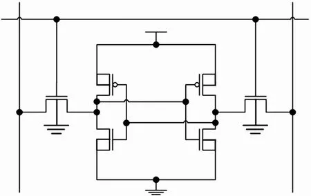
Fig.2.Schematics of 6-T SRAM cell.
3.Experimental results
The SNM of the SRAM cell is determined experimentally by measuring VTCs of the left hand and right hand inverters,as shown in Fig.3.Because SNM of a SRAM cell is defined as the side length of the square with the longest diagonal in closed regions of Fig.3(a),it is determined in a 45°rotated coordinate system(see Fig.3(b)).The left y axis of Fig.3(b)represents VTC of inverters rotated 45°with respect to the Fig.3(a)coordinate system,and the right y axis represents the difference between VTC rotated 45°.The maximum values of the right y axis in x axis intervals[?1,0]and[0,1]divided byare Data 1 and Data 0 SNM.Seen from Fig.3(b), both data sides’SNM are decreased by TID,which is different from the conclusion obtained in the old generation of devices that one data side’s SNM is decreased and the other data side’s SNM is increased.[3–8]

Fig.3.(color online)The tested SNM of SRAM cell pre and post TID.The black line represents data of pre irradiation and the red line represents data post 500 krad(Si).(a)Butterfly curves pre and post 500 krad(Si).(b)SNM estimation based on maximum squares in a 45° rotated coordinate system relative to panel(a).
Figure 4 shows the extracted ΔSNM from butterfly curves as a function of TID levels,which reveals that radiation has a larger effect on Data 0 than Data 1.As discussed in Sec.1, TID results in a preferred state and non-preferred state in the SRAM cell.

Fig.4.(color online)The extracted ΔSNM from butterfly curves as a function of TID levels.

Fig.5.(color online)The tested SNM of SRAM cell pre and post TID under different V dd.(a)Butterfly curves pre and post 500 krad(Si).The black line represents data of pre irradiation and the red line represents data post 500 krad(Si).(b)The extracted SNM change percentage as a function of TID levels under different V dd.
Vdddependence for the TID effect on SNM is shown in Fig.5.Seen from Fig.5(a),SNM under lower Vddis more sensitive to TID,as TID induced VTC negative shift is larger than higher Vdd.Figure 5(b)shows the extracted SNM change percentage as a function of TID levels under four different Vdd, indicating that TID effect on SNM is increased as Vdddrops.
4.Discussion
The mechanism of the TID effect on SNM is analyzed by measurement of Ids–Vgscurves of SRAM cell transistors.Figure 6 shows the influence of TID on Ids–Vgscurves of SRAM cell transistors.Except edge leakage,the threshold of 130 nm PD SOI n metal-oxide-semiconductor field effect transistor (NMOSFET)with ultra-thin gate oxide is negatively shifted by TID(easier to turn ON,see Fig.6(a)),but the mechanism is different from old generation devices with thick gate oxide. The threshold shift of 130 nm PD SOI NMOSFET is caused by radiation induced charges trapped in shallow trench isolation(STI)rather than in gate oxide for old generation devices.The minimum or nearly minimum-geometry transistors are commonly used in SRAM cells.The influence of TID induced charge trapped in STI on the electric potential of the body region cannot be ignored in minimum-geometry transistors.Therefore,the threshold of SRAM cell transistors will be impacted,known as the radiation induced narrow channel effect(RINCE).[14,15]Seen from Fig.6(a),TID induced drain current increase in NMOSFET can be divided into three regions.The drain current increase in Region I is caused by TID induced edge leakage.Edge leakage in narrow width NMOSFET is less affected by gate voltage,because it is brought about by TID induced charges trapped in the bottom of STI where the electric field applied by the gate voltage is very weak.In region III,the drain current increase is mainly caused by negative threshold shift,because the edge leakage is too small compared to the pre drain current.Region II is both affected by edge leakage and negative threshold shift.Known from Fig.6(b),the threshold of the pull-up p metal-oxide-semiconductor field effect transistor(PMOSFET) is positively shifted by RINCE(harder to turn ON).
Known from Fig.3,VTC negative direction shifts for left hand and right hand inverters result in a decrease of SNM.Wefind that VTC negative shift is closely related to drain current increase of pull-down NMOSFET at region Vgsfrom 0.3 V to 0.9 V.TID effect on SNM and Ids–Vgscurves of pull-down NMOSFET are shown in Fig.7.As discussed above,drain current increase of pull-down NMOSFET at region Vgsfrom 0.3 V to 0.9 V is caused by TID induced negative threshold shift.The switch point(VM)of VTC is determined by the threshold of pull-up PMOSFET and pull-down NMOSFET,as
where VTn(p),VDSATn(p),and Vn(p)are threshold voltage,saturation drain voltage,and width of pull-down(up)NMOSFET(PMOSFET),respectively.[16]The switch point of VTC will be negatively shifted by TID induced negative threshold shift in pull-down NMOSFET.Moreover,TID induced positive threshold shift in pull-up PMOSFET also makes the VTC have negative direction shifts,depending on the relationship between the switch point of the VTC and the transistor threshold.
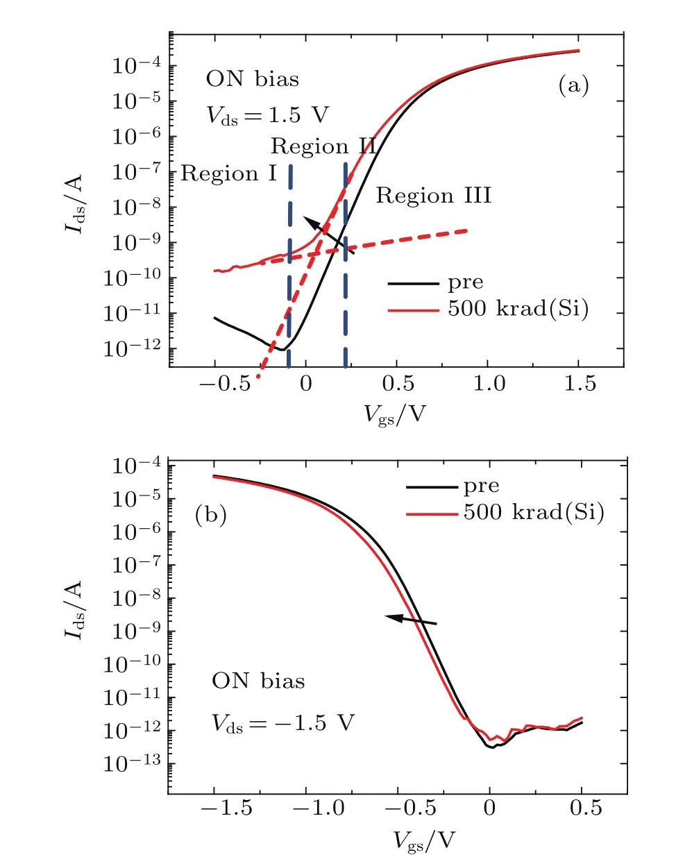
Fig.6.(color online)TID effect on I ds–V gs curves of SRAM cell transistors.(a)I ds–V gs curves of pull-down NMOSFET pre and post 500 krad(Si)of irradiation under ON bias.(b)I ds–V gs curves of pull-up PMOSFET pre and post 500 krad(Si)of irradiation under ON bias.
TID induced edge leakage in pull-down NMOSFET has a negligible influence on SNM.As shown in Fig.7,the high output voltage of the inverter almost has no change before and after TID.In spite of the resistance of off-state NMOSFET being decreased by TID induced edge leakage,it is still much larger than on-state pull-up PMOSFET due to its strong drive ability. The on-state current of pull-up PMOSFET is 1.06×10?5A, and off-state leakage of pull-down NMOSFET is increased to 7.96×10?10A after 500 krad(Si).As a result,the off-state leakage of NMOSFET is compensated by pull-up PMOSFET and only lower down a tiny output voltage.
Because BL and BLB are tied to 1.5 V,pass gate NMOSFETs(Q5 and Q6)are connected in parallel to pull-up PMOSFET.The low output voltage of the inverter will be pulled up by the TID induced edge leakage in pass gate NMOSFET. However,TID induced edge leakage in pass gate NMOSFETs is not large enough to induce an obvious output voltage rising, since pass gate NMOSFETs biases OFF or TG during irradiation,as shown in Fig.8.

Fig.7.(color online)SNM(left y axis)and I ds–V gs curves of pull-down NMOSFET(right y axis)pre and post 500 krad(Si)TID irradiation.

Fig.8.(color online)TID effect on I ds–V gs curves of pass gate NMOSFETs.(a)OFF bias.(b)TG bias.
TID induced asymmetry in SNM of 130 nm PD SOI SRAM cell is due to bias dependence of TID induced threshold shift in cell transistors.As shown in Fig.9,TID induced threshold shift is bias dependent and the effect of radiation is larger at ON bias both for NMOSFET and PMOSFET.Above bias dependence indicates that the change of right hand inverter VTC is mainly caused by NMOSFET Q2(see Fig.2), because it biases ON during TID irradiation.Accordingly,left hand inverter VTC shift is mainly caused by PMOSFET Q3 (see Fig.2).The left hand inverter VTC negative shift is larger than the righthand inverter,leading to a largerdecrease in Data 0 SNM,since radiation induced threshold shift in NMOSFET is larger than PMOSFET,as well as r in Eq.(1)is lower than 1 indicating that NMOSFET has a larger effect on VMthan PMOSFET when their threshold shift is the same.

Fig.9.(color online)Bias dependence of TID induced threshold shift in SRAM cell transistors.(a)Pull-down NMOSFETs.(b)Pull-up PMOSFETs.
Both data sides’SNM of 130 nm PD SOI SRAM cell are decreased,which is different from the conclusion obtained in old generation devices that one data side’s SNM is decreased and the other data side’s SNM is increased.The different bias dependence of TID induced threshold shift in PMOSFET is responsible for the above complicating conclusions.The threshold shift of OFF bias PMOSFET is larger than ON bias for the old generation device.[17]On the contrary,the effect of radiation is larger at ON bias for 130 nm PD SOI PMOSFET.Because NMOSFET and PMOSFET of old generation devices have a larger threshold shift in one side inverter of the SRAM cell,the VTC shift of one side inverter is much larger than the other side inverter.The VTC shift of the inverter with larger threshold shift plays a major role in SNM of SRAM cell,resulting in one increased SNM data side and the other decreased SNM data side,as shown in Fig.10.But for the 130 nm PD SOI device in this paper,NMOSFET with larger threshold shift is in another inverter from PMOSFET with larger threshold shift.Therefore,VTC shifts of both inverters are near and SNM of both data sides are decreased. The opposite bias dependence of TID induced threshold in old generation PMOSFET and 130 nm PD SOI PMOSFET can be explained by the electric field direction in oxide.For old generation PMOSFET,radiation induced charges are pushed to the upper interface of the gate oxide under ON bias,having less effect on the threshold than the bottom interface.While radiation induced charges in 130 nm PD SOI PMOSFET are pushed to the upper region of STI under ON bias,and only charges trapped in the upper region of STI have an effect on the threshold,so that the threshold shift of 130 nm PD SOI PMOSFET under ON bias is larger than OFF bias.

Fig.10.(color online)Schematic of TID effect on SNM of old generation SRAM.The black line represents VTC of pre irradiation and the red line represents VTC post irradiation.
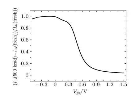
Fig.11.TID induced drain current increase in pull-down NMOSFET relative to fresh value changing with gate voltage.
Figure 11 shows TID induced drain current increase in pull-down NMOSFET relative to fresh value,which reveals that drain current under lower gate voltage is more sensitive to TID.Moreover,the V(Q)and V(QB)region of VTC (Vdd=0.9 V)affected by TID is from 0.2 V to 0.5 V(see Fig.5(a)),which is lower than VTC(Vdd=1.5 V).Therefore, TID induced SNM change under lower Vddis larger than that under high Vdd.
5.Conclusion
TID effect on 130 nm PD SOI SRAM cell stability is experimentally explored in this work.The SNM of the SRAM cell is directly measured by the test structure specifically designed for SNM testing.Experimental results show that both data sides’SNM are decreased due to the negative shift of VTC induced by TID,and TID has a larger effect on SNM of TID complement data.Moreover,Vdddependence was explored by measurement of SNM under different supply voltages changing with TID,and experimental result reveals that SNM under lower Vddis more sensitive to TID.The mechanism of the TID effect on SNM is analyzed by measurement of Ids–Vgscurves of cell transistors.The threshold shift of cell transistors caused by RINCE is responsible for the decreased SNM.Because NMOSFET and PMOSFET have larger threshold shift in different inverters,both data sides’SNM are decreased by TID rather than that one data side’s SNM being decreased and the other data side’s SNM being increased in old generation devices.SNM is more sensitive to TID under lower Vdd,since SNM under lower Vddis affected by the lower Vgsregion of Ids–Vgscurves of NMOSFET,and TID has a larger impact on the lower Vgsregion of Ids–Vgscurves.
[1]Seevinck E,List F J and Lohstroh J 1987 IEEE J.Solid-St.Circ.22 748
[2]Oldham T R and McLean F B 2003 IEEE T.Nucl.Sci.50 483
[3]Campbell A B and Stapor W J 1984 IEEE T.Nucl.Sci.31 1175
[4]Schott J T and Zugich M H 1987 IEEE T.Nucl.Sci.34 1404
[5]Bhuva BL,Johnson R L,Gyurcsik R S,Fernald KW,Kerns S E,Stapor W J,Campbell A B and Xapsos M A 1987 IEEE T.Nucl.Sci.34 1414
[6]Axness C L,Schwank J R,Winokur P S,Browwning J S,Koga R and Fleetwood D M 1988 IEEE T.Nucl.Sci.35 1602
[7]Stassinopoulos E G,Brucker G J,Gunten O V and Kim H S 1989 IEEE T.Nucl.Sci.36 2330
[8]Matsukawa T,Kishida A,Tanii T,Koh M,Horita K,Hara K,Shigeta B, Goto M,Matsuda S,Kuboyama S and Ohdomari I 1994 IEEE T.Nucl. Sci.41 2071
[9]Xiaoyin Y,Nathan H,Lawrence T C,Keith E H,David R A and Walter M S 2008 IEEE T.Nucl.Sci.55 3280
[10]Ding L L,Yao Z B,Guo H X,Chen W and Fan R Y 2012 J.Semeicond. 33 075010
[11]Zheng Q W,Yu X F,Cui J W,Guo Q,Ren D Y,Cong Z C and Zhou H 2014 Chin.Phys.B 23 106102
[12]Zheng Q W,Cui J W,Zhou H,Yu D Z,Yu X F,Lu W,Guo Q and Ren D Y 2015 Chin.Phys.B 24 106106
[13]King M P,Wu X,Eller M,Samavedam S,Shaneyfelt M R,Silva A I,Draper B L,Rice W C,Meisenheimer T L,Felix J A,Shetler K J, Zhang E X,Haeffner T D,Ball D R,Alles M L,Kauppila J S and Massengill L W 2017 IEEE T.Nucl.Sci.64 285
[14]Federico F and Giovanni C 2005 IEEE T.Nucl.Sci.52 2413
[15]Zhiyuan H,Zhangli L,Hua S,Zhengxuan Z,Bingxu N,Ming C,Dawei B and Shichang Z 2011 IEEE T.Nucl.Sci.58 1347
[16]Rabaey J M,Chandrakasan A and Nikolic B 2003 Digital Integrated Circuits-A Design Perspective(Upper Saddle River:Prentice-Hall) p.134
[17]Ma T P and Dressendorfer P V 1989 Ionizing Radiation Effects in MOS Devices and Circuits(New York:John Wiley and Sons)pp.256–333
28 April 2017;revised manuscript
12 June 2017;published online 31 July 2017)
10.1088/1674-1056/26/9/096103
?Project supported by the National Natural Science Foundation of China(Grant Nos.U1532261 and 11605282)and the Opening Fund of Key Laboratory of Silicon Device Technology,Chinese Academy of Sciences Research Projects(Grant No.KLSDTJJ2016-07).
?Corresponding author.E-mail:qiwinzheng@163.com,qwzheng@ms.xjb.ac.cn
?2017 Chinese Physical Society and IOP Publishing Ltd http://iopscience.iop.org/cpb http://cpb.iphy.ac.cn
猜你喜歡
中國核電(2021年3期)2021-08-13 08:56:36
中國臨床醫(yī)學影像雜志(2019年1期)2019-04-25 06:49:28
家庭影院技術(2018年11期)2019-01-21 02:20:52
紅土地(2018年12期)2018-04-29 09:16:48
華人時刊(2017年21期)2018-01-31 02:24:01
北方交通(2016年12期)2017-01-15 13:52:53
中國衛(wèi)生(2016年5期)2016-11-12 13:25:42
中國衛(wèi)生(2015年2期)2015-11-12 13:13:54
當代縣域經(jīng)濟(2015年12期)2015-03-20 15:51:06
創(chuàng)業(yè)家(2015年7期)2015-02-27 07:54:15

- Chinese Physics B的其它文章
- Relationship measurement between ac-Stark shift of 40Ca+clock transition and laser polarization direction?
- Air breakdown induced by the microwave with two mutually orthogonal and heterophase electric field components?
- Collective motion of active particles in environmental noise?
- Temperature dependence of heat conduction coefficient in nanotube/nanowire networks?
- Analysis of dynamic features in intersecting pedestrian flows?
- Heat transfer enhancement in MOSFET mounted on different FR4 substrates by thermal transient measurement?