Experimental and simulation studies of single-event transient in partially depleted SOI MOSFET?
2017-08-30 08:26:48WeiWeiYan閆薇薇LinChunGao高林春XiaoJingLi李曉靜FaZhanZhao趙發展ChuanBinZeng曾傳濱JiaJunLuo羅家俊andZhengShengHan韓鄭生
Chinese Physics B 2017年9期
關鍵詞:發展
Wei-Wei Yan(閆薇薇),Lin-Chun Gao(高林春),Xiao-Jing Li(李曉靜),Fa-Zhan Zhao(趙發展), Chuan-Bin Zeng(曾傳濱),?,Jia-Jun Luo(羅家俊),and Zheng-Sheng Han(韓鄭生)
1 Institute of Microelectronics,Chinese Academy of Sciences,Beijing 100029,China
2 Key Laboratory of Silicon Device Technology,Chinese Academy of Sciences,Beijing 100029,China
Experimental and simulation studies of single-event transient in partially depleted SOI MOSFET?
Wei-Wei Yan(閆薇薇)1,2,Lin-Chun Gao(高林春)1,2,Xiao-Jing Li(李曉靜)1,2,Fa-Zhan Zhao(趙發展)1,2, Chuan-Bin Zeng(曾傳濱)1,2,?,Jia-Jun Luo(羅家俊)1,2,and Zheng-Sheng Han(韓鄭生)1,2
1 Institute of Microelectronics,Chinese Academy of Sciences,Beijing 100029,China
2 Key Laboratory of Silicon Device Technology,Chinese Academy of Sciences,Beijing 100029,China
In this study,we investigate the single-event transient(SET)characteristics of a partially depleted silicon-on-insulator (PDSOI)metal-oxide-semiconductor(MOS)device induced by a pulsed laser.We measure and analyze the drain transient current at the wafer level.The results indicate that the body-drain junction and its vicinity are more SET sensitive than the other regions in PD-SOI devices.We use ISE 3D simulation tools to analyze the SET response when different regions of the device are hit.Then,we discuss in detail the characteristics of transient currents and the electrostatic potential distribution change in devices after irradiation.Finally,we analyze the parasitic bipolar junction transistor(p-BJT)effect by performing both a laser test and simulations.
single-event transient,pulsed laser,parasitic bipolar junction transistor,partially depleted silicon on insulator
1.Introduction
The development of silicon-on-insulator(SOI)devices has been motivated by the full dielectric isolation of individual transistors,which prevents the occurrence of latch-up.Moreover,because the concentration of sensitive charges that accumulate in SOI ICs is considerably less than that in bulksilicon integrated circuits(ICs)SOI ICs are less sensitive to single-event effects(SEE).[1–3]However,the parasitic bipolar junction transistor(p-BJT)effect inherent in the main metaloxide semiconductor(MOS)transistors reduces the hardness of the single-event upset(SEU)of SOI ICs,especially those ICs that utilize partially depleted silicon-on-insulator(PDSOI)technology.[4,5]
SET is a significant error mechanism in high-speed digital complementary MOS(CMOS)IC devices.[6,7]As the technology node and concomitant voltage scaling,SETs have become a contributor to the soft error rate for submicron devices. Particle accelerator testing is known as the standard method to be employed when characterizing the sensitivity of modern device technology to SEEs.[8]However,accelerator testing is usually expensive and is not easily accessible.For the past few years,pulsed laser systems have been widely used to characterize SEE behavior in semiconductor devices and logic ICs.[9–11]Studies have shown that pulsed laser excitation may be a reasonable approximation to ion excitation if the working wavelength could be chosen properly.[12]Recently,many local studies have been done on the SET characteristics of partially depleted(PD)-SOI MOSFETs.[13,14]Most of them analyze the SET characteristics using simulation tools,and few results have been obtained using pulsed laser systems.
This paper is arranged as follows.In Section 2,we describe the tested devices and the pulsed laser system.Then, in Section 3,we describe and analyze in detail the laser test results.We also discuss the sensitive region of PD-SOI devices.In Section 4,we use ISE simulation tools to analyze the SET response when different regions of the device were hit, and we also discuss the electric field distribution in the device at different times after irradiation.Finally,in Section 5,we conclude the paper.
2.Description of experiment setup
2.1.Experimental setup
The pulsed laser system used in this study is utilized at the Institute of Microelectronics,Chinese Academy of Sciences(IMECAS).Figure 1 illustrates the experimental setup of the pulsed laser system employed in our experiment.The laser beam is focused on the device with a 50×microscope objective,resulting in a 1.2-μm Gaussian spot with a 532-nm wavelength and 1-kHz repetition rate.As shown in Fig.1,the device-under-test(DUT)is fixed on a precise xyz stage to enable the DUT to move precisely.The DC-bias of the DUT is provided by Bias-T,and the SET waveform is captured and recorded by a 12.5GHz Tektronix oscilloscope.

Fig.1.(color online)Experimental configuration of(a)the pulsed laser system and(b)the system photo in IMECAS.
2.2.Tested devices
The transistors used in our experiment arentype devices because of the obvious SET response compared to P-type devices under the same radiation conditions.[15,16]These devices were fabricated at the IMECAS using 0.35-μm PD-SOI CMOS technology.As shown in Fig.2,the MOSFETs were processed on a UNIBOUND SOI substrate with an upper silicon film of 300 nm and a 400-nm-thick buried oxide(BOX) layer and the gate oxide thickness is close to 3 nm.The process involved CoSi2silicide,five layers of Aluminum metal, and shallow trench isolation(STI).
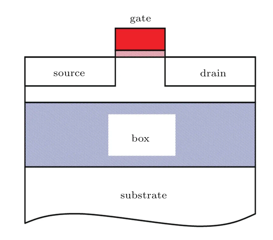
Fig.2.(color online)Physical structure of PD-SOI MOSFETs.
We applied two body contacts in the device structure at each edge along the gate width direction.The devices used in this experiment are irradiated in the off-state,with the drain biased at 3.3 V and other electrodes grounded.We tested two types of transistors,and the layouts are summarized in Fig.3.has a 0.35-μm long gate and a 1.05-μm wide channel,whilehas a 5-μm long gate and a 25-μm wide channel.

Fig.3.(color online)Layouts of(a) and(b)device 2;the laser hit locations are marked in layouts,and the markers do not represent the actual laser spot size(the body contacts are not shown).
3.Experimental results and discussion
The devices are scanned in the source-drain axis with a small displacement step by the pulsed laser(20 pJ).The laserhit locations are illustrated in the layout schematic in Fig.3.In order to test the SET sensitivity of,the metal space between the source and drain was increased to 10μm.De-in Fig.3(b)was designed to investigate the SET sensitivity of the body under the gate.

Fig.4.(color online)Variations of the transient currents when the laser hit different locations of device 1.
In Fig.4,as the laser moves towards the drain region, the peak amplitude of the transient current gradually increases. When location#6 is hit by a pulsed laser,the peak amplitude of the drain transient current reached 2.2 mA,which is the highest during the 9 locations.Considering the laser spot size and the device dimensions,#5–#6 are located in the vicinity of the body-drain junction.In the off-state,the body-drain junction of the device is reverse-biased,and the electrons induced by the pulsed laser could be quickly collected by the drain electrode with the help of the high electric field.On the other hand,the holes generated drift into the body region,and the source-body junction barrier is lowered.Then,the p-BJT effect is triggered,and results in the electrons from the source being injected into the body region and being collected by the drain effectively.In other words,the charges induced by the pulsed laser are amplified and the transient current increases largely.When the right-most drain region(#8–#9)is hit by the pulsed laser,the transient current remains at a relatively low level.The carriers generated here mostly recombine in the highly doped drain area,and only a small number of holes are collected by the doping gradient of the back interface of the drain.Then,these holes are swept to the body by the electricfield of the body-drain junction.However,the number of holes is not sufficient to trigger the p-BJT effect.When the left-most source region(#1–#2)is hit by the pulsed laser,some of the carriers are collected by the source,and the others mostly recombine during the diffusion process.In other words,only a small number of carriers generated in the source can diffuse to the drain.In general,fewer charges are collected when the drain or source region was hit.
The collected charge quantity measured on the drain when the laser strikes the nine locations inis shown in Fig.5(a).The charge collected by the drain electrode increased as the hit locations move towards the body-drain junction.Figure 5(b)shows the peak amplitude distribution of the drain transient current ofas a function of the laser hit position.We can clearly see that the body-drain junction area is more SET sensitive than the others.The cross section of PDSOI devices must include both the body under the gate and the drain region.Because the size of the laser spot is larger than the channel length of device 1,we cannot determine clearly the sensitivity of the body region.Therefore,we fabricatedwith a large channel length.
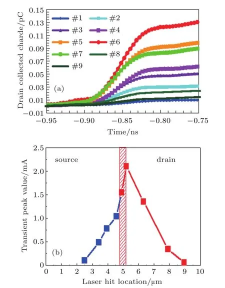
Fig.5.(color online)(a)Charge quantity calculated by integration of the transient current(b).The transient peak amplitude as a function of laser hit locations.
Figure 6(b)shows the collected charge quantity measured on the drain when the laser strikes the five locations in de-The charges collected also increase gradually with the laser moving towards the drain as.Moreover, the prompt response in Fig.6(b)indicates that when the laser strikes locations near the depletion region of the body-drain junction,the electrons can be rapidly collected by the electrode.

Fig.6.(color online)(a)Variations of the transient currents when the laser strikes different locations of(b)Charge quantity calculated by the integration of the transient current.
Reference[18]showed the solution to the diffusion equation of drain current I(t),and I(t)can be modeled as follows:

Equation(1)above shows that the drain transient current I(t) is proportional to the deposited charge Q,and is inversely proportional to L2,where L represents the bipolar base length and β is the bipolar gain.Here,the factors that influence I(t)have the same trend as in our description above.The bipolar base length ofis larger than that of device 1,and the drain transient current ofis clearly less.
We can conclude that the body-drain junction and its surroundings are more SET sensitive than the other regions in PD-SOI devices.When long-channel devices are hit by the pulsed laser,the body region near the source is less sensitive than the other short-gate devices.In order to further study the p-BJT effect,in the next section,we use the ISE TCAD simulation tools.
4.Simulation
In this section,we use ISE simulation tools to illustrate the phenomenon in the laser test experiment.We used a limited set of physical models to achieve a trade-off between a large realistic structure and an affordable simulation time.As the parasitic elements of the actual device are not considered, the simulated results may not be comparable with the experimental data.Instead,our goal is to qualitatively analyze the mechanism involved in the carrier transport process.The device used in the simulation has the same structure as the de-in the laser test experiment.
We used the Heavy Ion module in the ISE TCAD tool to simulate the charge-deposition process in the PD-SOI device.The linear energy transfer(LET)was characterized with the parameterwith a constant amplitude of 0.1 pc/μm. W used the Gaussian shape spatial distribution for the charge deposition process.
Figure 7 summarizes the drain transient currents when the heavy ion hit different locations.As heavy ions hit the vicinity of the body-drain junction,most of the charges are collected by the drain electrode.By comparison,the simulation result has the same trend as the laser test result.Although the charge generation mechanism of the pulsed laser is different for heavy ions,there is a large degree of similarity in terms of the charge collection and transport.
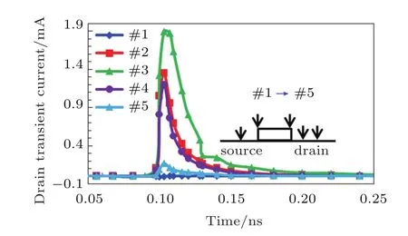
Fig.7.(color online)Variations of drain transient current when heavy ions strike different locations obtained during the simulation.
Figure 8 illustrates the transient currents measured at the source electrode when heavy ions hit different regions of the simulation device.When locations#2–#4 are hit,the source current in Fig.8 is first negative for several dozen picoseconds after irradiation,implying that the source electrode provides some electrons to the drain.In other words,the parasitic bipolar is triggered when heavy ions hit the vicinity of the bodydrain junction.After that,the source currents become positive, implying that bipolar amplification is over.Then,the charge collected by the source is from the excess electrons from the body,and the quantity is small.The bipolar amplification is maintained for 20 ps when heavy ions hit the body-drain junction,while it is maintained for 15ps for the others.

Fig.8.(color online)Variations of source transient current when heavy ions strike different locations obtained during the simulation.
Figure 9 shows the distributions of the electrostatic potential at different times when the body-drain junction(#3)is hit.Then,3 ps after the ion hits,the body potential increases to 2.5 V.As described above,the hole accumulation leads to an increase in the body potential.The source-body junction is forward biased and the p-BJT effect is triggered.After about 10ps,the potential disturbance begins to return to the original status which means that the charge amplification is over. This result is consistent with the source/drain current trend as shown in Figs.7 and 8.
From Fig.8,it is clear that the source current is nearly zero when the drain region(location#5)far from the body drain junction is hit.The p-BJT effect is not triggered at this time.Most holes generated at the drain region recombine here, and only a small part of the holes drift to the body.The source electrode could not collect any charges after irradiation.When the source region is hit,the source electrode only collects some electrons that are generated by diffusion,and the holes are finally evacuated by the body contacts.Figure 10 illustrates the distribution of the electrostatic potential at 3 ps when the source/drain region is hit.Compared to Fig.9,in both cases, there is no significant increase in the body potential after irradiation,which means that the parasitic effect is not triggered. Furthermore,it is clear that the ion irradiation only changes the source/drain potential.This result is consistent with the analysis above.
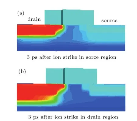
Fig.10.(color online)Distributions of electrostatic potential at 3 ps when (a)the source region(#1)and(b)drain region(#5)was hit(legend is the same as Fig.9).
After the simulation analysis,we can conclude that when the body-drain region and its vicinity are hit,the p-BJT effect is triggered,and the charges that are generated are amplified. The heavy-ion simulation and the pulsed laser test experiment have a large degree of similarity in terms of charge collection and transport.
5.Conclusion
In this paper,we studied the SET characteristics of PDSOI MOSFETs using the pulsed laser system and ISE 3D simulation tools.The experimental results obtained forindicate that the drain transient current reached the highest amplitude of 2.2 mA when the laser hit the body-drain region. For short-channel devices,both the body-under-gate and the drain region are sensitive to the SET effect.We found that the p-BJT effect amplifies the charges when sensitive regions are hit by the laser.3D simulation tools illustrate the transient currents collected by the source and drain.The transient current result obtained by performing the simulation has the same trend as that obtained with the laser experiment. Moreover,the body electrostatic potential distribution after irradiation confirmed that the increase in the body potential is caused by hole accumulation.The body-drain junction is the most sensitive region in PD-SOI MOSFETs,and the p-BJT effect should be minimized to decrease the SET current. These results have good practical significance for the study of radiation-hardening technology of other semiconductor devices and integrated circuits.
[1]Schwank J R,Ferlet-Cavrois V,Shaneyfelt M R,Paillet P and Dodd P E 2003 IEEE Trans.Nuc.Sci.50 522536
[2]Chou R,Kavalieros J,Doyle B,Murthy A,Paulsen N,Lionberger D, Barlage D,Arghavani R,Roberds B and Doczy M 2001 IEDM Tech. Dig.621
[3]Musseau O and Ferlet-Cavrois V 2001 NSREC short course
[4]AllesM L 1994 IEEE Trans.Nucl.Sci.41 2093
[5]AllesM L,Kerns S E,Massengill L W,Clark J E,Jones Jr K L and Lowther R E 1991 IEEE Trans.Nucl.Sci.38 1259
[6]Poivey C,Buchner S,Howard J and Label K 2016 Testing Guidelines for Single Event Transient(SET)Testing of Linear Devices
[7]Baumann R C 2005 Proc.IEEE Nuclear and Space Radiation Effects Conf.short course
[8]Melinger J S,Buchner S,Mcmorrow D,Stapor W J,Weatherford T R and Campbell A B 1994 IEEE Trans.Nuc.Sci.41 2582
[9]Buchner S,Kang K,Stapor W J,Campbell A B,KnudsonA R,Mcdonald P and Rivet S 1990 IEEE Trans.Nuc.Sci.NS-37 1825
[10]Musseau O,Ferlet-Cavrois V,Pelloie L,Buchner S,Mcmorrow D and Campbell A B 2000 IEEE Trans.Nuc.Sci.47 2197
[11]Ferlet-Cavrois V,Paillet P,Mcmorrow D,Fel N,Baggio J,Girard S, Duhamel O,Melinger J S,Gaillardin M,Schrank J R,Dodd P E, Shaneyfelt M R and Felix J A 2007 IEEE Trans.Nuc.Sci.54 2339
[12]Buchner S,Knudson A R,Kang K and Campbell A B 1988 IEEE Trans Nuc.Sci.NS-35 1517
[13]Zhang X C,Yue S G,Wang L and Li J C 2010 IIRW FINAL REPORT 149
[14]Zhuo Q Q,Liu H X and H Y 2012 Acta Phys.Sin.61 218501(in Chinese)
[15]Qin J R,Chen S M,Li D W,Liang B and Liu B W 2012 Chin.Phys.B 21 089401
[16]Kobayashi D,Saito H and Hirose K 2007 IEEE Trans.Nuc.Sci.54 1037
[17]Velacheri S,Massengill L W and Kerns S E 1994 IEEE Trans.Nuc. Sci.41 2104
[18]Fulkerson D E and Liu H 2004 IEEE Trans.Nuc.Sci.51 278
17 April 2017;revised manuscript
15 May 2017;published online 11 August 2017)
10.1088/1674-1056/26/9/098505
?Project supported by Funds of Key Laboratory,China(Grant No.y7ys011001)and Youth Innovation Promotion Association,Chinese Academy of Sciences (Grant No.y5yq01r002)
?Corresponding author.E-mail:chbzeng@ime.ac.cn
?2017 Chinese Physical Society and IOP Publishing Ltd http://iopscience.iop.org/cpb http://cpb.iphy.ac.cn
猜你喜歡
中國核電(2021年3期)2021-08-13 08:56:36
中國臨床醫學影像雜志(2019年1期)2019-04-25 06:49:28
家庭影院技術(2018年11期)2019-01-21 02:20:52
紅土地(2018年12期)2018-04-29 09:16:48
華人時刊(2017年21期)2018-01-31 02:24:01
北方交通(2016年12期)2017-01-15 13:52:53
中國衛生(2016年5期)2016-11-12 13:25:42
中國衛生(2015年2期)2015-11-12 13:13:54
當代縣域經濟(2015年12期)2015-03-20 15:51:06
創業家(2015年7期)2015-02-27 07:54:15

- Chinese Physics B的其它文章
- Relationship measurement between ac-Stark shift of 40Ca+clock transition and laser polarization direction?
- Air breakdown induced by the microwave with two mutually orthogonal and heterophase electric field components?
- Collective motion of active particles in environmental noise?
- Temperature dependence of heat conduction coefficient in nanotube/nanowire networks?
- Analysis of dynamic features in intersecting pedestrian flows?
- Heat transfer enhancement in MOSFET mounted on different FR4 substrates by thermal transient measurement?