Improved high-frequency equivalent circuit model based on distributed effects for SiGe HBTs with CBE layout?
2017-08-30 08:26:46YaBinSun孫亞賓XiaoJinLi李小進JinZhongZhang張金中andYanLingShi石艷玲
Chinese Physics B 2017年9期
Ya-Bin Sun(孫亞賓),Xiao-Jin Li(李小進),Jin-Zhong Zhang(張金中),and Yan-Ling Shi(石艷玲)
Shanghai Key Laboratory of Multidimensional Information Processing,Department of Electrical Engineering, East China Normal University,Shanghai 200241,China
Improved high-frequency equivalent circuit model based on distributed effects for SiGe HBTs with CBE layout?
Ya-Bin Sun(孫亞賓),Xiao-Jin Li(李小進)?,Jin-Zhong Zhang(張金中)?,and Yan-Ling Shi(石艷玲)
Shanghai Key Laboratory of Multidimensional Information Processing,Department of Electrical Engineering, East China Normal University,Shanghai 200241,China
In this paper,we present an improved high-frequency equivalent circuit for SiGe heterojunction bipolar transistors (HBTs)with a CBE layout,where we consider the distributed effects along the base region.The actual device structure is divided into three parts:a link base region under a spacer oxide,an intrinsic transistor region under the emitter window, and an extrinsic base region.Each region is considered as a two-port network,and is composed of a distributed resistance and capacitance.We solve the admittance parameters by solving the transmission-line equation.Then,we obtain the small signal equivalent circuit depending on the reasonable approximations.Unlike previous compact models,in our proposed model,we introduce an additional internal base node,and the intrinsic base resistance is shifted into this internal base node, which can theoretically explain the anomalous change in the intrinsic bias-dependent collector resistance in the conventional compact model.
SiGe heterojunction bipolar transistors(HBT),small-signal equivalent circuit,distributed effects, CBE layout
1.Introduction
In recent years,SiGe heterojunction bipolar transistors (HBTs)have undergone rapid growth because of their high speed,high driving power,and low noise,and they have been applied to fields such as wireless communication,analog circuit,fast data acquisition,and conversion.[1–3]Small-signal equivalent circuit models,such as the lumped SGP,VBIC, HICUM,and Mextram,are often used to characterize transistor performance,optimize the device structure,and guide circuit design.[4–6]However,bipolar transistors are actually large distributed networks that are composed of a basic resistance and capacitance,and their design is not always as easy as described in the above lumped models.Although most transistor electrical performances can be effectively characterized by lumped models,there remain fundamental limitations with respect to actual device structures.[7]When extracting the small-signal model parameters in conventional Mextram,we find that the bias-dependent collector epilayer resistance RC1C2monotonously decreases as the base voltage VBCincreases, which clearly deviates from basic device physics theory,and the underlying physical mechanism should therefore be investigated.
Owing to its special base structure,SiGe HBTs show a built-in multi-Mrad total dose hardness with no intentional hardening.[8–10]However,single-event effects(SEE)remain a serious problem,with recent results demonstrating a low linear energy-transfer threshold and high saturated cross sections.[11–14]A reduction in the sensitive area enclosed by deep trench isolation is considered an effective method of improving the net upset cross section.Therefore,a transistor with minimum feature size,i.e.,using only a single collector,base, and emitter(CBE)contacts,possesses a high SEE immunity, compared with standard devices with double collector and base contacts(CBEBC).[11,12]Furthermore,when the transistors are exposed to the space-energetic particle environment, the distributed effect is more significant because the irradiation damages are generally not uniformly distributed throughout the whole transistor structure.[8]Therefore,it is necessary to investigate the small-signal equivalent circuit based on the distributed effects for SiGe HBTs with a CBE layout.
In the present work,in order to determine the physical mechanisms by which the extracted RCCdecreases as VBCincreases,we propose an improved small-signal equivalent circuit that is based on the distributed effects for SiGe HBTs with a CBE layout.The whole transistor is divided into three parts along the base region.Then,we obtain the high-frequency equivalent circuit under the cut-off mode by solving transmission line equations,and taking into account the distributed effects.The intrinsic base resistance RBIis pushed into the internal base node,and the added component of RBI(CTE+CTC)/3CTCis found to contribute to the declinedRCCas VBCincreases.Finally,we obtain the equivalent circuit in the forward-active mode by adding four additional modules into the equivalent circuit in the cut-off states.
2.Background
The conventional hybrid-.π small-signal equivalent circuit for SiGe HBTs under forward-active mode is depicted in Fig.1,as adopted in HICUM or Mextram.The collector series resistance and base series resistance are separately divided into two parts:a constant external part RCXand intrinsic bias-dependent epilayer resistance RC1C2,a constant external resistance RBX,and a variable intrinsic resistance RBI.
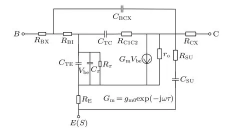
Fig.1.Conventional small-signal equivalent circuit for SiGe HBTs.

Fig.2.Extracted collector epitaxy layer resistance R C1C2 as a function of V BC.
As demonstrated in our previous study,the small-signal model parameters can be precisely extracted based on the nonlinear rational function fitting.[15]However,we observed an abnormal variation of the collector epilayer resistance RC1C2, and it decreases as the base voltage VBCincreases,as shown in Fig.2.It appears that this variation deviates from basic device physics theory,and RC1C2is actually expected to increase as VBCdecreases.According to the cross-sectionalview of the intrinsic transistor under the emitter window,as shown in Fig.3, the depletion width WBCnarrows as VBCincreases,and this is because of the decreased reverse bias voltage.Consequently, the width of the neutral collector region WCKincreases,causing an increase in RC1C2.

Fig.3.(color online)A simplified cross-sectional view of the intrinsic transistor.
Therefore,in the conventional compact model,the obtained RC1C2contradicts basic device physics theory.In order to find the underlying physical mechanism,starting with the actual device structure,we propose an improved high frequency small-signal equivalent circuit for SiGe HBTs based on the distribution effects.The intrinsic base resistance RBIis pushed into the introduced internal base node,and contributes to the collector resistance with certain proportion,and this can fundamentally explain the above abnormal variation of RC1C2versus the base voltage VBC.
3.Device-under-test and method for the proposed model
The device evaluated in this work features a single-stripe CBE configuration,i.e.,with only one CBE,as opposed to the larger CBEBC stripe configuration.The typical cross-section is shown in Fig.4.The key process includes an n?collector epitaxy,a graded SiGe base epitaxy,an in-situ doped polysilicon emitter,LOCOS isolation,an n+collector sinker,and an ion-implanted extrinsic base.Along the base region,the whole transistor structure is divided into three parts:I)a link base region including the spacer oxide,II)an intrinsic transistor region,and III)an extrinsic BC junction containing metal silicide.
In the present work,we separately determine the small signal equivalent circuit under the cut-off and forward-active mode.Each region is considered as a two-port network composed of several basic resistors and capacitors.We obtained the admittance parameters by solving the transmission line equation,and we then determine the small-signal equivalent circuit in the cut-off mode depending on some reasonable approximations,using the well-known π network characteristics,[16]as shown in Fig.5.Finally,we directly obtained the equivalent circuit in forward-active mode by adding four additional modules.
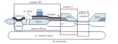
Fig.4.(color online)Schematic cross-section for SiGe HBT with a single-stripe CBE structure.
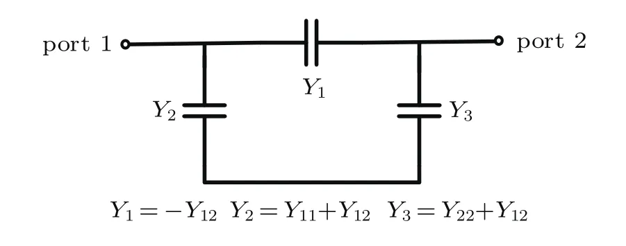
Fig.5.The well-known characteristics of the π network.
4.Results and discussion
4.1.Equivalent circuit under cut-off mode
4.1.1.Link-base region
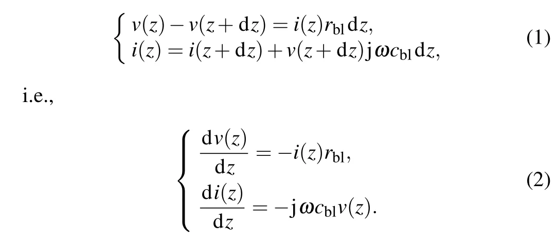
As depicted in Fig.4,the link-base region contains only the BCjunction,and the distributed network is shown in Fig.6, where rblis the series-base resistance and cblis the shunt BC junction capacitance per unit length.We assume that all of the electrical elements along the link-base region are distributed uniformly.The total length of this region is assumed to be d.
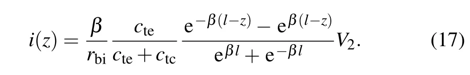
To determine the current i(z)and voltage v(z)at any position z,we have the following equation:
Combined with the boundary conditions v(0)=V1and v(d)= V2,the general solution of Eq.(2)along the transmission line is given as
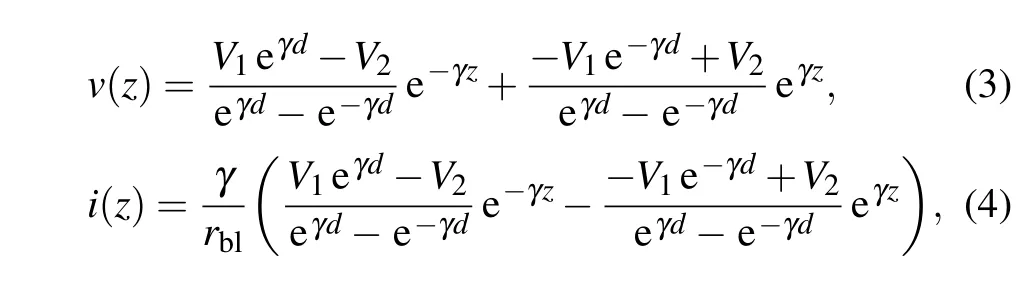
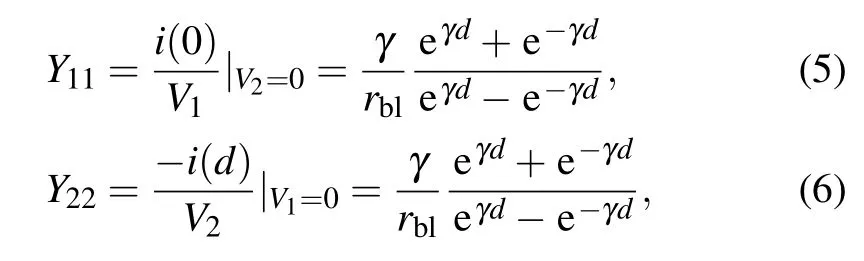
and the two transfer admittances are:
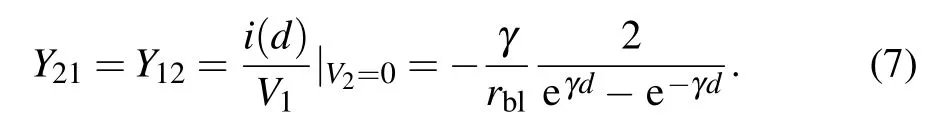
Then we can obtain the following equations:

With respect to Fig.5,it is difficult to directly determine the equivalent circuit according to Eqs.(8)and(9).It is necessary to approximate the exponential term e±γdusing the Taylor series.Obviously,the more items taken in the Taylor series expansion,the more accurate will be the obtained equivalent circuit;however,the obtained equivalent circuit may be more complicated.Considering the trade-off between the accuracy and complexity,here,we approximated e±γdas a third-order Taylor expanded formula
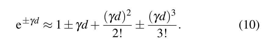
Then,substituting Eq.(10)into Eqs.(8)and(9),we obtain
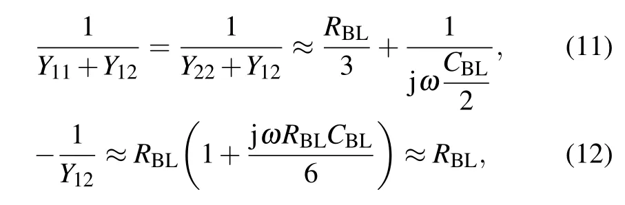
where RBL=d rbland CBL=d cblseparately represent the total series resistance and shunt capacitance for the link-base region.Then,the equivalent circuit for the link-base region of the SiGe HBT with the CBE layout can be simplified in the following form in Fig.7.
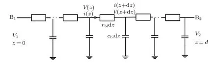
Fig.6.Distributed network for the link-base region in the cut-off mode.
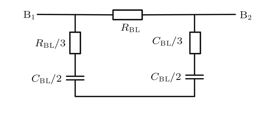
Fig.7.Simplified equivalent circuit for the link-base region of the SiGe HBT with the CBE layout.
4.1.2.Intrinsic transistor region
The distributed network for the intrinsic transistor region is shown in Fig.8.Similar to the link-base region,we assume that the electrical parameters along the length direction are distributed uniformly.The series-intrinsic base resistance, BE junction,and BC junction shut capacitance per unit length are set as rbi,cte,and ctc,respectively.The total length of the intrinsic transistor is set as l.
Fig.8.Distributed network for the intrinsic transistor region under cut-off mode.
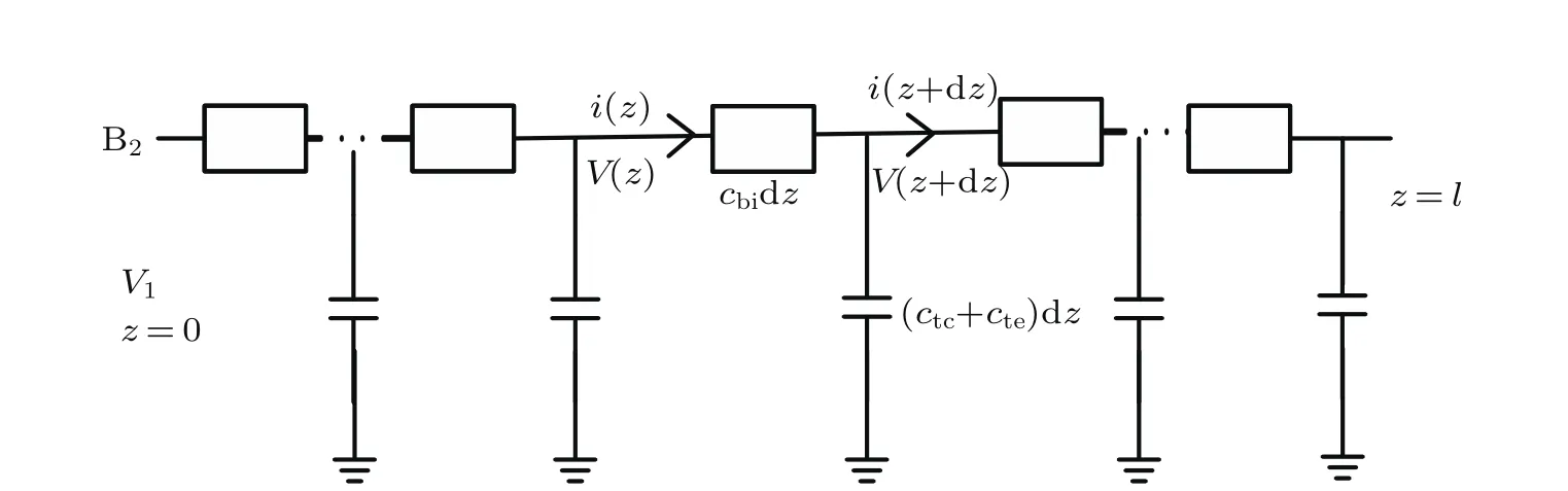
Fig.9.Equivalent distributed network of intrinsic transistor for solving Y11 and Y12,where the emitter terminal is connected to ground and the base terminal B1 is the applied voltage V1.
First,we determine Y11and Y21for the two-port network in Fig.8.The base terminal B2and emitterterminal E1are separately applied to voltage V1and ground(here V2=0).Then, we reduce the distributed network to the form in Fig.9.With boundary conditions v(0)=V1,i(l)=0 and the similar approaches to the solution,Y11and Y21are written as
Next,we obtain the admittance parameter Y22.Now, we apply emitter terminal E1to V2,and base terminal B2is grounded.The current i(z)and voltage v(z)at arbitrary position z satisfies the following equation:
Considering the boundary conditions v(0)=0 and i(l)=0, the voltage v(z)and current i(z)along the intrinsic base region are determined by
We assume thatiB2and iE1represent the current flowing into terminals B2and E1,anditcis the total current flowing into ground through ctc.According to Kirchhoff’s law,there existsiB2+iE1=itc,where

where CTC=ctcl,CTE=ctel,and RBI=rbilare the total intrinsic BC junction capacitance,intrinsic BE junction capacitance,and intrinsic base resistance,respectively.Then,the distributed network of the intrinsic transistor is equivalent to that in Fig.10.

Fig.10.Simplified equivalent circuit for the distributed network of the intrinsic transistor region.
4.1.3.Extrinsic base region
A heavily doped poly-silicon and metalsilicide with a low sheet resistance are generally employed in modern advanced SiGe HBT technology.[2]Consequently,the extrinsic base resistance RBXis significantly reduced,and is much smaller than RBLand RBI.Therefore,the distributed effect in the extrinsic base region is not obvious.For simplicity,the extrinsic base region is represented by a lumped parallel RC network, as shown in Fig.11,where CBCXis the extrinsic BC junction capacitance.
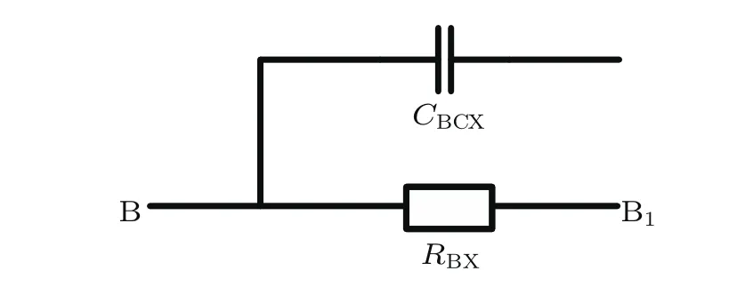
Fig.11.Simplified equivalent circuit for the extrinsic base region.
4.1.4.Equivalent circuit model for the whole transistor in cutof fmode
Once the equivalent-circuit of the link-base region,intrinsic transistor region,and extrinsic base region are determined by solving the transmission-line equation,we obtain the following hybrid-.π small-signal equivalent circuit for SiGe HBTs with a CBE layout under cut-off mode,as shown in Fig.12.The parasitic emitter resistances and collector resistances are treated as lumped elements that depend on the device geometry.The series-collector resistance contains two parts:a constant external part RCXand an intrinsic bias dependent part RC1C2.In addition to a simple substrate network,we adopted a parasitic substrate resistance RSUin series with the substrate-collector junction capacitance CSUand CTSto model the substrate characteristics.[16]
Compared to the conventional MEXTRAM and HICUM, the high-frequency small-signal equivalent circuit presented in this work introduces an additional circuit node B2,which separates the intrinsic base resistance RBIand the link-base resistance,RBL.Furthermore,the intrinsic base resistance RBIis shifted into the internal node B2and separately contributes to the emitter resistance and collector resistance with various proportions.As marked within the dashed-line box,the admittance Y1can be approximately rewritten as
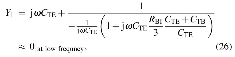
which means that the marked network can be considered open and removed from the small-signal equivalent-circuit at low frequency.Hence the component of RBI(CTE+CTC)/3CTCis directly added to the intrinsic bias-dependent collector resistance RC1C2,and it is regarded as a total equivalent resistanceIt is the added component of RBI(CTE+CTC)/3CTCthat can fundamentally explain why the collector epitaxial collector resistance decreases as VBCincreases.As VBCincreases,the BC junction depletion width decreases,and then the width of the neutral base region increases owing to a decreased reverse bias voltage.The base current flows parallel with the BC junction and is perpendicular to the direction of the base width.Therefore,the increased neutral base width leads to a reduction of the intrinsic base resistance RBI.Considering the large ratio of(CTE+CTC)/CTC, the decreased RBIcauses the collector resistance R′C1C2to decrease as VBCincreases.
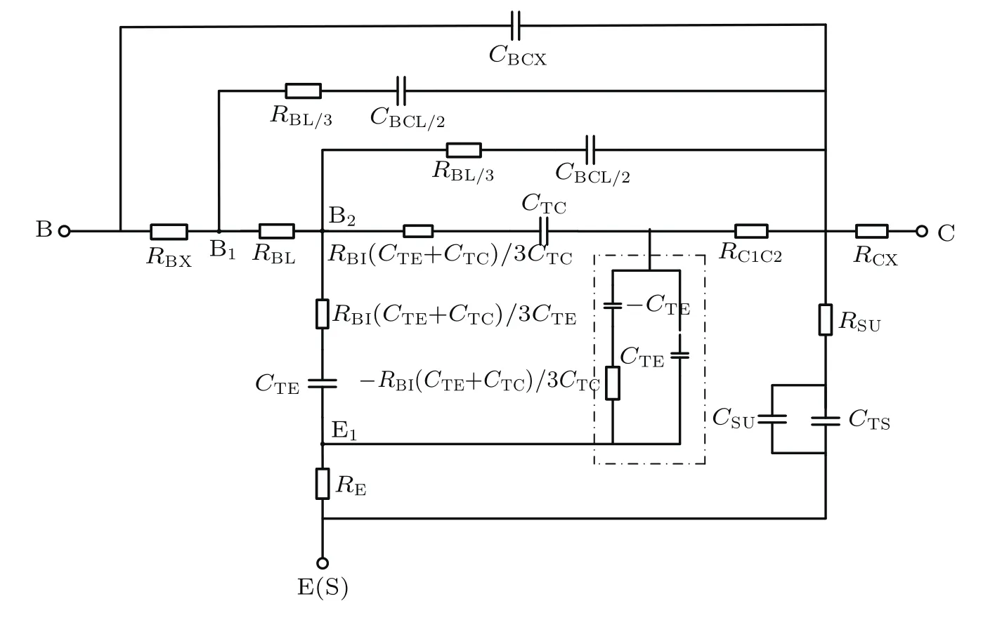
Fig.12.Improved small-signal equivalent circuit for SiGe HBT with CBE layout in cutoff mode.
4.2.Equivalent circuit in forward-active mode
Generally,in order to achieve the current amplification, SiGe HBTs are usually biased in the forward-active mode with a common-emitter configuration.As shown in Fig.13,the corresponding small-signal equivalent circuit can be easily obtained based on the result of the cut-off mode.Because the BE junction is forward-biased,for simplicity,two elements,the junction diffusion capacitance Cπand the junction diffusion resistance Rπ,are added in parallel with the BE junction depletion capacitance CTE.We used Cπand Rπto characterize the response of the BE junction to an applied low-frequency small-signal sinusoidal voltage,and their values are functions of the BE junction current.Cπreflects the ability of charge storage in the base region as a function of vbe,and Rπreflects the modulation effect of the emitter voltage on the base current.The voltage-dependent current GmVbeis the collector current in the transistor,and it is controlled by the internal voltage Vbe.Gmmodels the modulation effect of the base voltage on the collector current.The output resistance rois primarily due to the Early effect.[7]In the future,we will focus on the model parameter extraction for our proposed model.

Fig.13.Improved small-signal equivalent-circuit model for SiGe HBT in the forward-active mode.
Theoretically,the proposed small-signal model is still applicable when the SiGe HBT operates under very high frequency because the proposed model is based on the high frequency distributed effects.The whole transistor is considered as a large distributed network consisting of basic elements,such as a resistance,a capacitance and a diode.In fact,the proposed model should also be verified by performing simulations or experiments.The verification process generally includes two parts:parameter extraction from the measured results,and a comparison between the measured and simulated (in ADS)results.However,the parameter extraction process is relatively complicated and we are in the process of achieving this task.Details about the parameter extraction and the verification process will be included in our following work
5.Conclusion
This paper presents a novel high-frequency small-signal equivalent-circuit for SiGe HBTs with a CBE layout,and is based on the distributed effects in an actual device structure. According to the base region position,the whole transistor is divided into three parts:a link-base region,an intrinsic transistor region,and an extrinsic base region.We obtained the Y parameters for each region by solving the transmission line equation.We obtained the small-signal equivalent circuit in the cut-off and forward-active mode using the well known π network characteristics under reasonable approximations.The proposed equivalent circuit model can fundamentally explain the anomalous variations that exist between the bias-dependent collector resistance and the base voltage in conventional compact models.In the future,we aim to focus on the parameter extraction for our proposed model.
[1]Schmid R L,Song P,Coen C T,Ulusoy A C and Cressler J D 2014 IEEE Trans.Microw.Theory Tech.62 2755
[2]Avenier G,Ribes G,Montagne A,Canderle E,Celi D and Derrier N 2014 IEEE International Electron Devices Meeting(IEDM)3.9.1
[3]Pekarik J J,Adkisson J,Gray P,Liu Q,Camillo-Castillo R and Khater M 2014 IEEE Bipolar/BiCMOS Circuits and Technology Meeting (BCTM)92
[4]McAndrew C,Seitchik J and Bowers D 1995 IEEE Bipolar/BiCMOS Circuits and Technology Meeting(BCTM)170
[5]Schr?ter M and Chakravorty A 2010 Compact Hierarchical Modeling of Bipolar Transistors with HICUM(Singapore:World Scientific)
[6]Van D T R,Paasschens J C J and Kloosterman W J 2012 The Mextram Bipolar Transistor Model level 504.11.0.Delft University of Technolog
[7]Cressler J D 2008 Measurement and Modeling of Silicon Heterostructure Tayloramp;Francis Group,LLC
[8]Sun Y B,Fu J,Xu J,Wang Y D,Zhou W and Zhang W 2014 Chin. Phys.B 23 0116104
[9]Li P,Guo H X,Guo Q,Zhang J X,Xiao Y,Wei Y and Cui J W 2015 Chin.Phys.B 24 088502
[10]Sun Y B,Fu J,Xu J,Wang Y D,Zhou W and Zhang W 2016 Chin. Phys.B 25 048501
[11]Sutton A K,Bellini M,Cressler J D,Pellish J A,Reed R A and Marshall P W 2007 IEEE Trans.Nucl.Sci.6 2044
[12]Krithivasan R,Marshall P W,Nayeem M,Sutton A K,Kuo W and Haugerud B M 2006 IEEE Trans.Nucl.Sci.53 3400
[13]Reed R A,Marshall P W,Pickel J C,Carts M A,Fodness B and Niu G F 2003 IEEE Trans.Nucl.Sci.50 2184
[14]Marshall P W,Carts M A,Campbell A,McMorrow D,Buchner S and Stewart R 2000 IEEE Trans.Nucl.Sci.47 2669
[15]Sun Y B,Fu J,Xu J,Wang Y,Zhou W and Zhang W 2015 Superlattices and Microstructures 80 11
[16]Chen H,Chen K,Huang G and Chang C 2006 IEEE Trans.Electron Devices 9 2287
23 March 2017;revised manuscript
2 June 2017;published online 31 July 2017)
10.1088/1674-1056/26/9/098502
?Project supported by the National Natural Science Funds of China(Grant Nos.61574056 and 61504156),the Natural Science Foundation of Shanghai, China(Grant No.14ZR1412000),Shanghai Sailing Program,China(Grant No.17YF1404700),and the Science and Technology Commission of Shanghai Municipality,China(Grant No.14DZ2260800).
?Corresponding author.E-mail:xjli@ee.ecnu.edu.cn
?Corresponding author.E-mail:jzzhang@ee.ecnu.edu.cn
?2017 Chinese Physical Society and IOP Publishing Ltd http://iopscience.iop.org/cpb http://cpb.iphy.ac.cn

- Chinese Physics B的其它文章
- Relationship measurement between ac-Stark shift of 40Ca+clock transition and laser polarization direction?
- Air breakdown induced by the microwave with two mutually orthogonal and heterophase electric field components?
- Collective motion of active particles in environmental noise?
- Temperature dependence of heat conduction coefficient in nanotube/nanowire networks?
- Analysis of dynamic features in intersecting pedestrian flows?
- Heat transfer enhancement in MOSFET mounted on different FR4 substrates by thermal transient measurement?