Lowering the driving voltage and improving the luminance of blue fluorescent organic light-emitting devices by thermal annealing a hole injection layer of pentacene?
2017-08-30 08:26:50JianGao高建QianQianYu于倩倩JuanZhang張娟YangLiu劉洋RuoFeiJia賈若飛JunHan韓俊XiaoMingWu吳曉明YuLinHua華玉林andShouGenYin印壽根
Chinese Physics B 2017年9期
Jian Gao(高建),Qian-Qian Yu(于倩倩),Juan Zhang(張娟), Yang Liu(劉洋),Ruo-Fei Jia(賈若飛),Jun Han(韓俊), Xiao-Ming Wu(吳曉明),?,Yu-Lin Hua(華玉林),?,and Shou-Gen Yin(印壽根),§
1 School of Materials Science and Engineering,Tianjin University of Technology,Tianjin 300222,China
2 Key Laboratory of Display Materials and Photoelectric Devices,Ministry of Education,Tianjin 300222,China
3 Tianjin Key Laboratory of Photoelectric Materials and Devices,Tianjin 300222,China
Lowering the driving voltage and improving the luminance of blue fluorescent organic light-emitting devices by thermal annealing a hole injection layer of pentacene?
Jian Gao(高建)1,2,3,Qian-Qian Yu(于倩倩)1,2,3,Juan Zhang(張娟)1,2,3, Yang Liu(劉洋)1,2,3,Ruo-Fei Jia(賈若飛)1,2,3,Jun Han(韓俊)1,2,3, Xiao-Ming Wu(吳曉明)1,2,3,?,Yu-Lin Hua(華玉林)1,2,3,?,and Shou-Gen Yin(印壽根)1,2,3,§
1 School of Materials Science and Engineering,Tianjin University of Technology,Tianjin 300222,China
2 Key Laboratory of Display Materials and Photoelectric Devices,Ministry of Education,Tianjin 300222,China
3 Tianjin Key Laboratory of Photoelectric Materials and Devices,Tianjin 300222,China
We chose pentacene as a hole injection layer(HIL)to fabricate the high performance blue fluorescent organic light emitting devices(OLEDs).We found that the carrier mobility of the pentacene thin films could be efficiently improved after a critical annealing at temperature 120°C.Then we performed the tests of scanning electron microscopy,atomic force microscopy,and Kelvin probe to explore the effect of annealing on the pentacene films.The pentacene film exhibited a more crystalline form with better continuities and smoothness after annealing.The optimal device with 120°C annealed pentacene film and n-doped electron transport layer(ETL)presents a low turn-on voltage of 2.6 V and a highest luminance of 134800 cd/m2at 12 V,which are reduced by 26%and improved by 50%compared with those of the control device.
organic light-emitting device(OLED),annealing,pentacene film,hole injection
1.Introduction
The organic light-emitting diodes(OLEDs)have now been accepted as a dream display owing to their attractive features such as high display quality,slim body,flexibility,low power consumption,and so on.[1–4]Improving their electroluminescent(EL)performance is a primary goal in the development of technological applications.Since OLEDs can potentially be used in portable and wearable electronic devices, the researchers are also interested in the low driving voltage devices based on the point of view of energy saving.Hence, lots of studies have focused on thin films treatments and the exploitation of organic materials for low driving voltage and high luminance.[5–7]Currently,several methods for reducing the driving voltage of OLEDs have been reported.Introducing a p-type or n-type doping structure in the charge transport layer is the most commonly used method.[8–10]However,the co-evaporation process is complicated,and the minor doping ratio is inaccurate to control.It is worth mentioning that inserting an injection layer between the electrode and the organic layer is easy and effective.[11–13]
It is well known that an effective injection layer requires appropriate energy level matching and high carrier mobility.[14]As a p-type material,pentacene is one of the most promising organic semiconductors due to its high mobility and stability,which has been widely used in organic field effect transistors(OFETs).[15,16]Furthermore,some works on OLEDs comprising pentacene thin films have also been reported previously.Shi et al.[17]reduced the hole injection by introducing pentacene thin films to balance the recombination of electrons and holes,which improved the efficiency of the OLEDs.We hope that a pentacene thin film can function as an effective hole injection layer(HIL)in OLED with high carrier injection ability to improve the performance of the OLED.By investigation,the carrier mobility of the pentacene thin film can be improved through thermal annealing in OFETs.[15,18]
In this work,we introduce this method to the OLEDs and reveal that relatively high annealing temperature could induce pentacene to develop into high crystallinity films with highlyordered,large-sized,and smooth shape.As an HIL in OLEDs, the annealed pentacene film will be used to improve the hole injection ability at a low driving voltage.Simultaneously,the n-doped electron transport layer(ETL)will also be adopted to balance the hole–electron pairs in the emission layer(EML), which results in high luminance and low driving voltage for OLEDs.
2.Experiment
2.1.Device fabrication
The cleaning of the ITO glass substrate with a sheet resistance of 20 ?/sq is subsequently performed with detergent, deionized water,acetone,and is opropanol in an ultra-sonic bath for 10 min each.After drying,the surface of ITO is treated under UV/O3for 15 min.All organic films are deposited on a pre-cleaned ITO glass substrate using a thermal evaporation of BOC Edwards Auto 500 thermal evaporation system in an M.Braun 20 G glove box with a deposition rate of 2 nm/min,and an in-situ quartz crystal is used to monitor the thickness of the vacuum depositions. Figure 1 shows the principle scheme of the OLED.Fluorescent blue dye N6,N6,N12,N12-tetrap-tolylchichrysene-6, 12-diamine(DNCA)doped into a host material 9,10-Di(2-naphthyl) anthracene(ADN)serves as the emission layer (EML),which is sandwiched between the hole transport layer (HTL)of N,N’-Bis-(1-naphthalenyl)-N,N’-bis-phenyl-(1,1’-biphenyl)-4,4’-diamine(NPB)and the electron transport layer (ETL)of 4,7-diphnenyl-1,10-phenanthroline(Bphen).A pentacene film is introduced as an HIL.
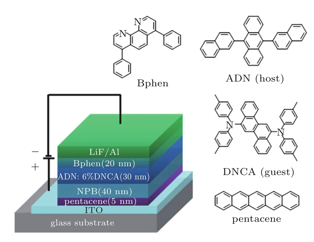
Fig.1.(color online)Principle scheme of an OLED.
2.2.Annealing conditions and test instruments
The thermal annealing tests were carried out in a vacuum oven(VC 20,M.BRAUN).The samples were kept for 1 h at different temperatures(such as 100°C,120°C,and 150°C). The OLED performance measurements were carried out using a Keithley 2400 source and a PR650 scan spectrometer in a glove box.We characterized the surface morphology and crystallinity of the deposited pentacene films by using atomic force microscopy(AFM,Bruker Innova),scanning electron microscopy(SEM,Rigaku D/max 2500),and x-ray diffraction (XRD,Hitachi SU8010).The energy levels were measured by a Kelvin probe(KP020).
3.Results and discussion
The EL characteristics of the pentacene-based OLEDs with different annealing temperatures were investigated.The structures of different devices are listed as follows:
A:ITO/NPB(40 nm)/ADN:DNCA(30 nm, 6 wt.%)/Bphen(20 nm)/LiF(0.8 nm)/Al(120 nm);
B:ITO/pentacene(5 nm)/NPB(40 nm)/ADN:DNCA (30 nm,6 wt.%)/Bphen(20 nm)/LiF(0.8 nm)/Al(120 nm); the structures of devices C,D,and E are the same as that of device B(pentacene with out annealing),except for the pentacenefilms annealed at different temperatures at 100°C,120°C,and 150°C.
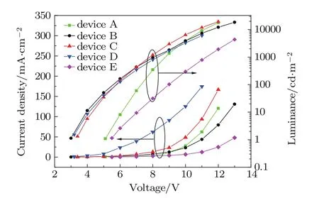
Fig.2.(color online)Current density–luminance–voltage characteristics of devices A–E.
From Fig.2,it can be found that the current density of device B is lower than that of device A at the same bias.That is to say,the insertion of the pentacene film does not improve the hole injection ability of the OLEDs,which is probably because the pentacene film appears as a grain of amorphous phase.When the thickness of the pentacene film is thin,the vacancies and defects exist in the film,which results in a reduced injection current at a constant voltage.[18]However,the current density of devices B–D is improved with the increase of the annealing temperature,and device D shows the highest current density under the same driving voltage.It is worth mentioning that the current density of device E obviously decreases when the annealing temperature reaches 150°C.By inspecting the change of J–V curves,we find that appropriate heat treatment of the pentacene thin films(device D)may improve the hole injection ability in the OLEDs.But we alsofind that the brightness of device D is not increased significantly.So the effect of annealing on the pentacene films needs to be further investigated.
Here we explored the morphology,roughness,work function of the pentacene films through a series of tests.Figure 3 shows the SEM images of the pentacene thin films obtained under different annealing conditions(without annealing,100°C,120°C,and 150°C annealing).From Figs.3(a)–3(c),with the increase of the annealing temperature,the pen-tacene films become more ordered,large-sized,and smooth. However,voids appearing in Fig.3(d)apparently break the continuity of the thin films,which may account for the decrease of the current density of device E with 150°C annealing.Among these images,the pentacene film in Fig.3(c) presents the best continuities and smoothness.

Fig.3.SEM images showing the morphology of the pentacene films:(a)without annealing sample,(b)100°C annealed sample,(c) 120°C annealed sample,(d)150°C annealed sample.
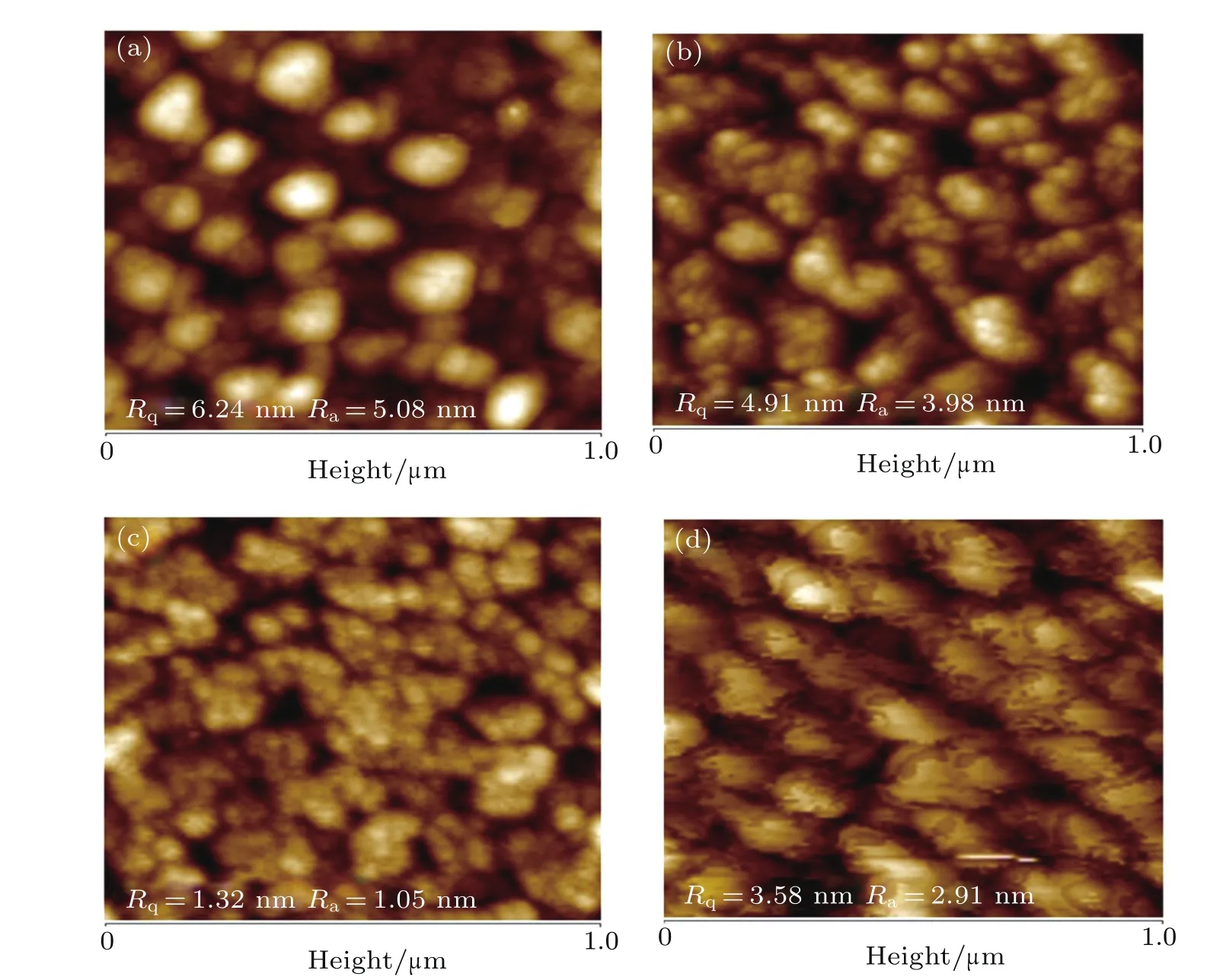
Fig.4.(color online)AFM images(1μm×1μm)of 5 nm pentacene thin films on ITO/glass:(a)before and(b)–(d)after annealing (100°C,120°C,and 150°C).
Figure 4 shows the AFM topographic images of the pentacene thin films before and after annealing at 100°C,120°C, and 150°C.In Fig.4(a),many small projections are observed, and the bright parts are probably a grain of the bulk phase pentacene.[19,20]More bright parts disappear as the temperature increases.When the temperature reaches 120°C,some adjacent grains join together,which suggests that local recrystallization has occurred due to the annealing(Fig.4(c)).However,from Fig.4(d),150°C annealing causes such a desorption effect that the thin film has been undermined.Moreover, from the roughness data labeled on the AFM images,the lowest roughness(Ra=1.32 nm,Rq=1.05 nm)of the pentacenefilm is obtained under the annealing of 120°C.
To confirm the formation of the crystallinity for the pentacene film and the improvement of the hole injection ability, further exploration is provided through the measurements of XRD and Kelvin probe.Figure 5 shows the XRD patterns of the pentacene films before and after annealing at 100°C, 120°C,and 150°C.
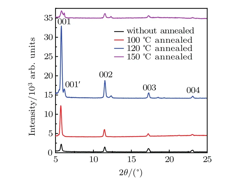
Fig.5.(color online)XRD patterns of the pentacene films on sapphire substrate before and after annealing(100°C,120°C,and 150°C).The thickness of the pentacene film is 50 nm.
The intensity of the(001)diffraction peak from the thinfilm phase of the non-annealed pentacenefilm is relatively low. When the annealing temperature reaches 120°C,the intensity of the(001)peak becomes markedly stronger,and a series of (00k)peaks related to the crystalline structure of pentacene are observed.It can be attributed to the fact that some adjacent pentacene grains join together via a recrystallization process under the annealing of 120°C.Furthermore,120°C annealing also facilitates the pentacene molecules to form the bulk phase which is corresponding to the(001′)peak at 6.18°.[19]The bulk phase of pentacene indicates that the adhesion between pentacene and ITO is improved.[21–23]Thus the pentacene film forms a crystalline shape,which optimizes the interface contact between ITO and pentacene molecules.Meanwhile the defects in the pentacene grains could be repaired under appropriate thermal annealing.With the temperature increasing to 150°C,the intensities of the(00k)peaks are significantly reduced,which indicates that the crystalline structure of pentacene has been damaged.
Figure 6 shows the work function of the pentacene films under various conditions(without annealing,100°C, 120°C,and 150°C annealed).The average values of work function under the conditions are?5.0280 eV,?5.0175 eV,?4.9854 eV,and?5.0489 eV,respectively.Among these values,the highest work function of the pentacene film is obtained when the annealing temperature reaches 120°C,which will be beneficial for the hole injection from ITO to HIL. The energy level diagram of pentacene inserted between ITO and NPB is shown in Fig.7,the highest occupied molecular orbital(HOMO)levels of pentacene and ITO are?5.0 eV and?4.7 eV,respectively.The hole injection barrier at pentacene(annealing at120°C)/ITOinterface is 0.2854 eV,which is 0.0426 eV lower than that of pentacene(without annealing)/ITO.The results provide solid evidence that the 120°C annealed pentacene film can lower the hole injection barrier and improve the hole transport ability under a certain bias.
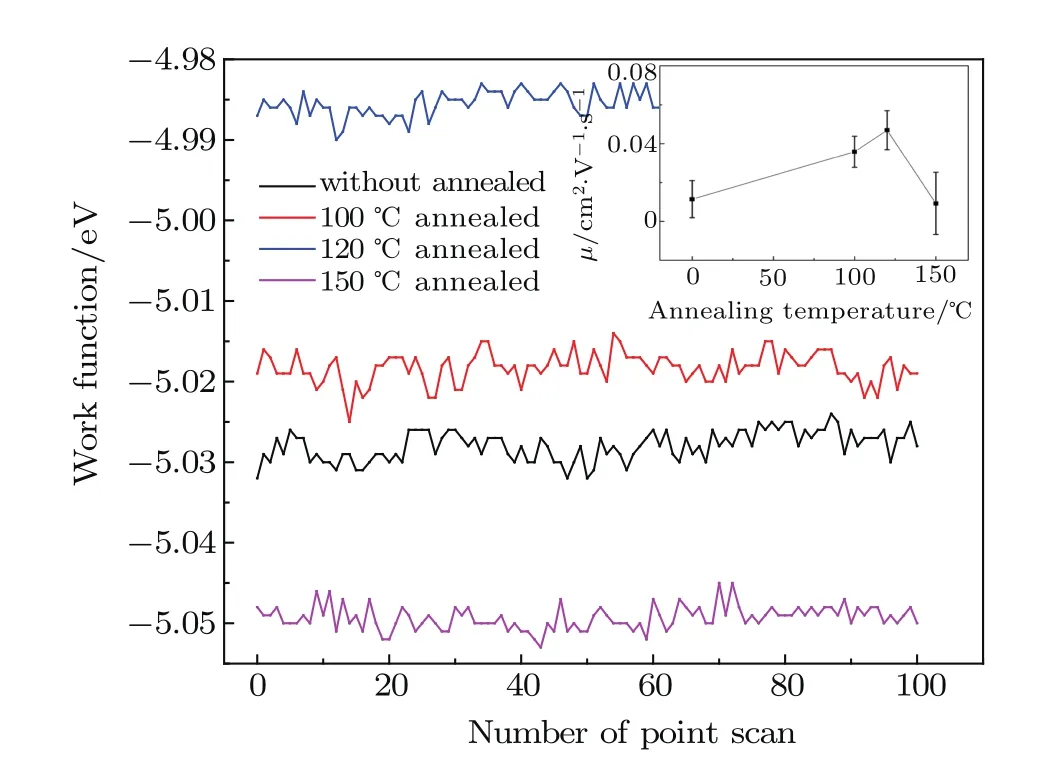
Fig.6.(color online)The work function of the pentacene films with different annealing conditions measured by a Kelvin probe(film prepared on the ITO glass substrate with a thickness of 5 nm).Inset shows the carrier mobility of the OFETs based on the pentacene films annealed at different temperatures.
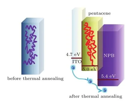
Fig.7.(color online)Energy levels and hole injection diagram of the device.
Moreover,the carrier mobility of the pentacene films annealed at different temperature was measured by organic field effect transistors.The inset of Fig.6 shows the change in carrier mobility as a function of annealing temperature.The carrier mobility of the device without thermal annealing is about 1.15×10?2cm2/V·s.When the annealing temperature reaches 120°C,the pentacene film exhibits a more crystalline form with best continuities and smoothness,which is beneficial to improving the carriermobility(4.69×10?2cm2/V·s)of the device.Considering the p-type character of pentacene,the results indicate that the hole transport ability of the pentacenefilm will also be improved with an optimal annealing temperature.
The current density of device D has been improved markedly based on the enhancement of the hole injection ability.However,the brightness of device D is not improved obviously as expected.As is known,the total current density of OLEDs is equal to the current density of the injected electrons from the cathode plus the part of the hole current density flowing to the anode without recombination.[24–26]The injected electrons from the cathode into the EML can be considered as the same due to the equal electrons injection barrier for these devices.However,the current density of device D is higher than that of device B,which results from excessive holes disrupting the balance of recombination.That is to say,excessive holes accumulated in the EML induce exciton quenching.The fraction of hole current density reaching the counter electrode without recombination in device D is higher than that of device B.The unbalanced number of electrons and holes injected into the EML would affect the efficiency and luminance of the devices.To improve the performance of the OLED,the electron injection and transport ability should be enhanced.So we introduced an n-doping ETL in the OLED to enhance the electron transport ability,and further discussed the effect of charge balance.
To prove the above theory,we fabricated another group of OLEDs named devices 1–5.The only difference compared to the previous devices is that we replaced the Bphen(20 nm) by Bphen(10 nm)/Bphen:Mg(10 wt.%,10 nm).As shown in Fig.8,there is an obvious increase in luminance and current density of device 4 compared with those of devices 1 and 2 at the same driving voltage.

Fig.8.(color online)The EL characteristics of devices 1–5:(a)current density–luminance–voltage characteristics,(b)current efficiency–power efficiency–current density characteristics.
Table 1 shows the EL performances of devices 1–5. Through the annealing of the pentacene film,the turn-on voltage and the driving voltage are reduced to 2.6 V and 5.1 V for device 4,which have been reduced by 35%and 20%compared with those of device 1.As the voltage increases to 12 V,device 4 presents a very high luminance of 134800 cd/m2,whereas devices 1 and 2 show the luminance of 92120 cd/m2and 89810 cd/m2.The luminance improvement at a constant currentdensity corresponds to the increased current efficiency and power efficiency.As seen from Fig.8,combining the 120°C annealed pentacene film and the n-doped ETL structure,the hole and electron injection abilities have been simultaneously improved.The balanced hole–electron pairs are beneficial for exciton’s formation under a low driving voltage,which results in the EL performance improvement of the OLEDs.

Table 1.The EL performances of the OLEDs.
4.Conclusion
We use a simple approach to effectively improve the EL performance of the blue fluorescent organic light-emitting device by introducing the annealed pentacene film as the hole injection layer.The pentacene film can form a highly-ordered, large-sized and smooth lamellar shape after a critical annealing at temperature 120°C,which could induce the pentacene molecules to develop into a high crystallinity film and improve the hole transport ability of the devices.Furthermore, combined with an n-doped ETL,the electron transport ability has been enhanced so as to improve the charge balance in the EML,which results in a high luminance and a low driving voltage of OLEDs.The optimal OLED(device 4)exhibits a low turn-on voltage of 2.6 V and a driving voltage of 5.1 V at 1000 cd/m2,which are obviously reduced by 0.9 V and 1.4 V respectively compared with those of the control device. Meanwhile,this device also presents a very high luminance of 134800 cd/m2at 12 V,which is 1.5 times higher than that of the control device.These results indicate that this simple and effective approach may fulfill the requirements of OLED with low driving voltage and high luminance.
[1]Zhang Q S,Li B,Huang S,Nomura H,Tanaka H and Adachi C 2014 Nat.Photon.8 1
[2]Cao J,Jiang X Y and Zhang Z L 2006 Appl.Phys.Lett.89 252108
[3]Luo J,Li X Z,Hou Q,Peng J B,Yang W and Cao Y 2007 Adv.Mater. 19 1113
[4]Miao Y Q,Gao Z X,Zhang A Q,Li Y H,Wang H,Jia H S,Liu X G and Tsuboi T 2015 Chin.Phys.B 24 057802
[5]Hu Y,Zhou D Y,Wang B,Wang Z K and Liao L S 2016 Appl.Phys. Lett.108 153303
[6]Zhang Q S,Li J,Shizu K,Huang S,Hirata S,Miyazaki H and Adachi C 2012 J.Am.Chem.Soc.134 14706
[7]Udagawa K,Sasabe H,Cai C and Kido J 2014 Adv.Mater.26 5062
[8]Wemken J H,Krause R,Mikolajick T and Schmind G 2012 J.Appl. Phys.111 074502
[9]Nikiforov G O 2016 Org.Electron 36 120
[10]Zhou D Y,Zu F S,Zhang Y J,Shi X B,Aziz H and Liao L S 2014 Appl.Phys.Lett.105 083301
[11]Zhang X W,You F J,Zheng Q H,Zhang Z L,Cai P,Xue X G,Xiong J and Zhang J 2016 Org.Electron 39 43
[12]Siemund H and G?bel H 2016 IEEE Trans.Electron Devices 63 3700
[13]Takada M,Furuta S,Kobayashi T,Nagase T,Shinagawa T,Lzaki M and Naito H 2016 J.Appl.Phys.120 185501
[14]Qian L,Zheng Y,Choudhury K R,Bera D,So F,Xue J and Holloway P H 2010 Nano Today 5 384
[15]Xiang L Y,Wang W and Gao Feng Li 2016 IEEE Trans.Electron Devices 63 4440
[16]Raghuwanshi V,Bharti D,Varun I,Mahato A K and Tiwari S P 2016 Org.Electron 34 284
[17]Shi S W and Ma D G 2005 Semicond.Sci.Technol.20 1213
[18]Guo D,Ikeda S,Saiki K,Miyazoe H and Terashima K 2006 J.Appl. Phys.99 094502
[19]Ahn T,Jung H,Suk H J and Yi M H 2009 Synth.Met.159 1277
[20]Dinelli F,Murgia M,Biscarini F and De Leeuw D M 2004 Synth.Met. 146 373
[21]Fukuda K,Sekitani T and Someya T 2009 Appl.Phys.Lett.95 023302
[22]Ji T,Jung S and Varadan V K 2008 Org.Electron 9 895
[23]Fukuda K,Yokota T,Kuribara K,Sekitani T,Zschieschang U,Klauk H and Someya T 2010 Appl.Phys.Lett.96 053302
[24]Zhang F J,Xu Z,Zhao S L,Zhao D W,Yuan G C and Cheng Z M 2008 Appl.Surf.Sci.255 1942
[25]Park Y W,Choi H J,Choi J H,Park T H,Jeong J W,Song E H and Ju B K 2012 IEEE Electron Device Lett.33 1156
[26]Yun C,Cho H,Kang H,Lee Y M,Park Y and Yoo S 2009 Appl.Phys. Lett.95 053301
7 March 2017;revised manuscript
22 May 2017;published online 18 July 2017)
10.1088/1674-1056/26/9/098507
?Project supported by the National Natural Science Foundation of China(Grant No.60906022),the Natural Science Foundation of Tianjin,China(Grant No.10JCYBJC01100),the Key Science and Technology Support Program of Tianjin,China(Grant No.14ZCZDGX00006),and the National High Technology Research and Development Program of China(Grant No.2013AA014201).
?Corresponding author.E-mail:wxm@tjut.edu.cn
?Corresponding author.E-mail:yulinhua@tjut.edu.cn
§Corresponding author.E-mail:sgyin@tjut.edu.cn
?2017 Chinese Physical Society and IOP Publishing Ltd http://iopscience.iop.org/cpb http://cpb.iphy.ac.cn

- Chinese Physics B的其它文章
- Relationship measurement between ac-Stark shift of 40Ca+clock transition and laser polarization direction?
- Air breakdown induced by the microwave with two mutually orthogonal and heterophase electric field components?
- Collective motion of active particles in environmental noise?
- Temperature dependence of heat conduction coefficient in nanotube/nanowire networks?
- Analysis of dynamic features in intersecting pedestrian flows?
- Heat transfer enhancement in MOSFET mounted on different FR4 substrates by thermal transient measurement?