
10Gb/s transmit equalizer using duobinary signaling over FR4 backplane①
2017-09-25 12:53:30ZhangYinhang張銀行HuQingsheng
High Technology Letters 2017年3期
關鍵詞:銀行
Zhang Yinhang (張銀行), Hu Qingsheng
(Institute of RF- & OE-ICs, Southeast University, Nanjing 210096, P.R.China)
10Gb/s transmit equalizer using duobinary signaling over FR4 backplane①
Zhang Yinhang (張銀行), Hu Qingsheng②
(Institute of RF- & OE-ICs, Southeast University, Nanjing 210096, P.R.China)
A 10Gb/s 6-tap transmit equalizer based on partial response signaling for high speed backplane transmission is presented. By combining features of equalizer and frequency-dependent channel, duobinary signaling can be generated at the output of FR4 backplane, aiming at increasing data rate while reducing design complexity. Based on 0.18μm CMOS technology, this equalizer has been designed and fabricated, in which both variable capacitor and load resistor calibration techniques are explored to eliminate the effect of process variations. The chip occupies 0.68×0.8mm2including I/O pads and consumes a power of 194mW with 1.8V power supply. Measurement results show that a typical 3-level eye diagram can be obtained at the receiver and the equalizer can work properly at the data rate of 10Gb/s.
transmit equalizer, duobinary, partial response, load resistor calibration, CMOS technology
0 Introduction
The demand for high performance data communication over backplane and chip-to-module has been increasing dramatically. When data rate increases, received data will be seriously damaged and the signal integrity will be severely impaired due to dielectric loss proportional to the frequency and skin effect which is proportional to the square root of the frequency. To enhance signal integrity, the most commonly used equalization techniques for high-speed backplane include decision feedback equalization (DFE) and feed-forward equalization (FFE), either in receiver or in transmitter. DFE is a nonlinear equalization technique and has some drawbacks such as error propagation. Apart from it, DFE can only compensate postcursor inter symbol interference (ISI) while FFE can compensate both postcursor and precursor. As a linear equalizer, FFE is normally designed as a FIR filter and can be used in high speed serial link due to its simplicity and good performance[1-3].
With the rapid increase of data rate, however, traditional non-return-zero (NRZ) based equalizer faces more and more challenges due to the limitation of process. To alleviate the problem, alternative modulations such as PAM4 and duobinary are adopted to reduce the bandwidth requirement effectively. It has been known that a 3-level modulation duobinary can reduce the bandwidth requirement to half of that for NRZ and has a bandwidth requirement on par with PAM4 which is a 4-level modulation scheme. It is obvious that duobinary and PAM4 modulation outperform NRZ in bandwidth requirement of transceiver.
Because of its 4 levels, however, the receive system for PAM4 is more complex compared to that of duobinary signal. In addition, for the same average signal power and channel noise, the signal integrity of PAM4 is far more vulnerable to deterioration when compared with that of duobinary[4].
Motivated by increasing data rate while reducing design complexity, this work explores a transmit equalizer based on partial response signal, i.e. duobinary signaling. Different from typical equalizer which compensates the loss of channel as much as possible, this equalizer just needs to compensate channel loss partially and make the output of channel be a duobinary signal. More importantly, the feature of band-limited channel can be used in generating duobinary signals.
1 Architecture design
From the view of timing, duobinary signaling firstly proposed by Lender allows controlled amount of inter symbol interference and can be expressed as the sum of current bit and the former one as following:
y(n)=x(n)+x(n-1)
(1)
where, y(n) and x(n) are the output and input at time n, respectively, and x(n-1) is the input at time n-1. It indicates that a duobinary signal can be generated with ease by adding adjacent pulse responses whose spacing is one symbol[5].
The working principle of the equalizer will be analyzed first from the view of frequency domain. See Fig.1, a typical frequency-dependent channel has a roll-off that is much steeper than that of desired duobinary signal. As a result, the proposed equalizer which is in fact an equalization filter should have appropriate high-frequency boost to generate a duobinary signal at the end of channel. However, the amount of high-frequency boost is significantly reduced when compared to NRZ signaling since the duobinary frequency spectrum has a null at half the bit rate, providing a distinct advantage. In other words, by the combination of the channel response and the FIR filter, required duobinary response can be realized[6].
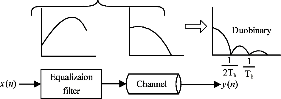
Fig.1 Working principle of the proposed equalizer

Fig.2 Block diagram of the proposed filter
To realize the equalization filter with high frequency boost, a 6-tap FIR filter with 5 delay units is designed in this paper, shown as Fig.2. Its output can be expressed as
(2)
where Vinis the input, Ci(i=-3,-2,…,2) is the ithtap coefficient, and T is the period of one symbol. From Fig.2, it can be seen that the input and its delay signals are multiplied by Cifirst and then summed together. After that, the summed current is converted to the output voltage Voutby the load resistors. It is obvious that a desired performance of the filter can be acquired by optimizing the delay unit and the value of tap coefficients[7].
2 Circuit design
2.1 Delay unit
The delay line plays an important role in the filter and can be realized as a passive pattern or an active one. In our design an active structure is employed since it is invulnerable to process variation and occupies less area when compared to a passive one. The active delay line, however, is difficult to meet the bandwidth requirements for 10Gb/s data rate especially in 0.18μm CMOS technology. Consequently, a structure with source degeneration capacitance is employed to expand the bandwidth. See Fig.3, the transfer function of the delay unit can be given as

(3)
where Gm3is the transconductance of M3, CLis the load capacitance and CSis the source degeneration capacitance. It can be observed that there are two poles: p1=(GmRS+2)RSCS, p2=1/CLRLand one zero z1=2/(RSCS). If z1is placed in front of p1and p2, the circuit will be peaked and the purpose of expanding the bandwidth can be realized. Practically, the position of the zero is adjusted by changing the bias voltage of variable capacitor CS[8,9].

Fig.3 Delay unit with source capacitive degeneration
2.2 Delay line optimization using calibration techniques
As mentioned above, the accuracy of delay line is important to the performance of filter. Below the delay circuit from the view of group delay will be analyzed and optimized. The group delay of the proposed delay unit can be expressed as

(4)
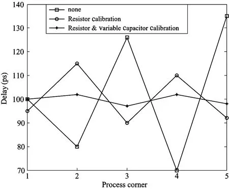
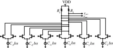
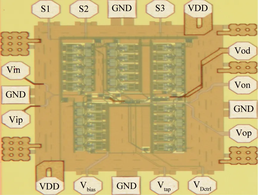
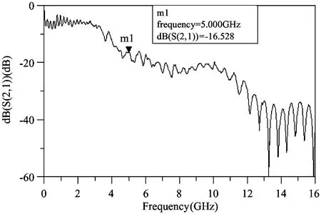
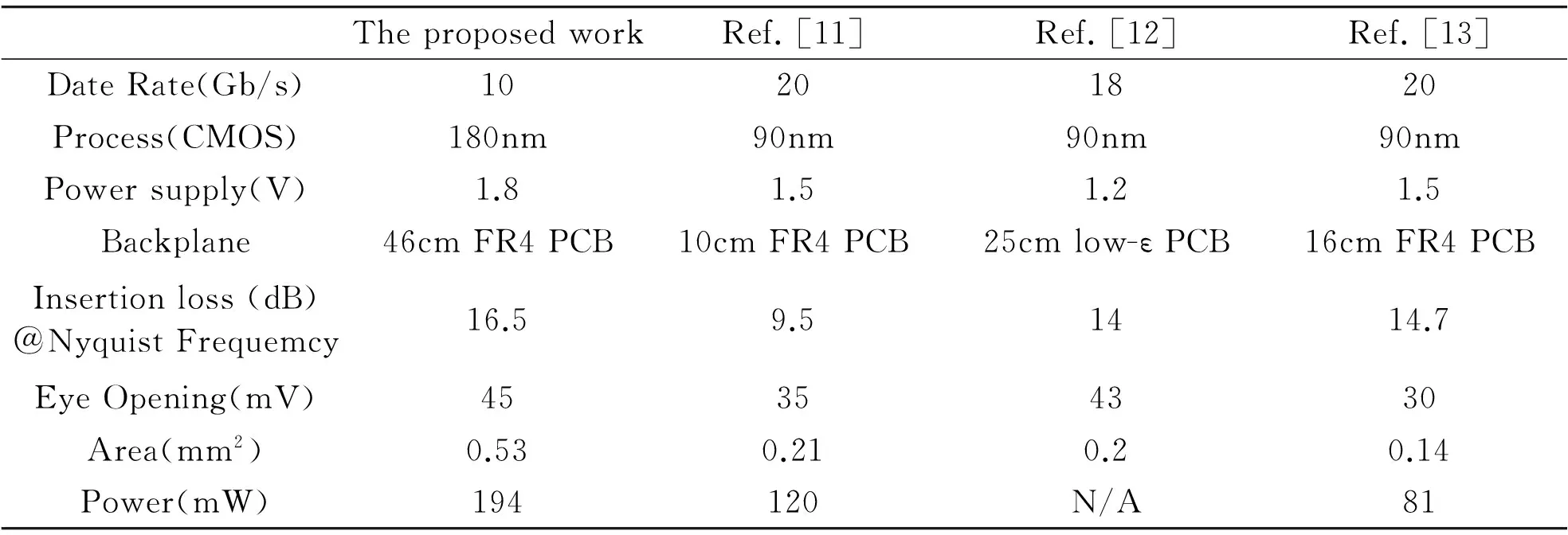
When frequency is low(w< (5) It can be inferred from Eq.(5) that the group delay is closely related to the zero. When CSbecomes large, the group delay is small, and vice versa. Thus, changing the capacitance of CSby Dctrl, the location of z1can be adjusted and the desired delay time can be obtained. This can be illustrated further in Fig.4, which gives the group delay versus Dctrl. It can be viewed that the group delay is more sensitive to Dctrlat low frequency. When the frequency goes high, however, the method of variable capacitor calibration is not effective, even worsens the flatness of group delay and leads to non-uniformity of bandwidth. This is because in this case both pole and zero will change with the process corner. Thus, making variable the two resistors RLand RSwhich determine the poles will allow improving the flatness of group delay at high frequency. This technique is also known as resistor calibration. Fig.4 Group delay of the delay line Fig.5 indicates the approach of resistor calibration in detail, in which load resistor RLis replaced by shunt branches of resistors in series with PMOS switches S1~S3. Meanwhile, source resistance RSis also replaced by shunt branches of resistors in series with NMOS switches T1~T3which are logic reverse of S1~S3. Using this resistor calibration technique, delay variations due to PVT (process, voltage, temperature) can be reduced effectively. It is worth noting that the resistance of each branch should be less than 15% of the total resistance in order to acquire high calibration accuracy and linearity. Fig.5 Delay unit with resistor calibration Fig.6 shows the simulation result of delay time of the delay unit under different process corners. It can be observed that the flatness of the delay time is improved greatly by using capacitor and resistor calibration technique. Fig.6 Delay time under different process corners 2.3 Multiplier-summer In this study, a multiplier-summer is designed based on current mode logic (CML), shown as Fig.7. It can be seen that the input signal Vinand its delay versions are summed first in the form of current and then converted to the output voltage Voutthrough load resistance RL. The output voltage can be expressed as Vout=[Gm-3Vin(t+3T)+Gm-2Vin(t+2T) +Gm-1Vin(t+T)+GmVin(t) +Gm+1Vin(t-T)+Gm+2Vin(t-2T)]RL=[C-3+C-2+C-1+C0+C1+C2]ISSRL (6) where Gmi(i=-3,-2,…,2) are the input transconductances, Ci(i=-3,-2,…,2) are the tap coefficients and C0ISSis the current of the main tap. Fig.7 CML based multiplier & summer To obtain the optimal Ci, zero-forcing algorithm is used as (7) where, x-5~x5are the precursors and postcursors of channel pulse response which can be obtained by inversing Fourier transformation of the measured S-parameter, and vector [0 0 1 1 0 0]Tis the target of equalization. In this way, the optimal value [C-3C-2C-1C0C1C2]Tcan be found[10]. The equalizer has been fabricated using 0.18μm CMOS process. Fig.8 gives the die photograph of the chip which has an area of 0.68×0.8mm2including I/O pads. An on-chip measurement is performed, in which the input of the chip is a 300mV 10Gb/s PRBS23 differential signal and its output is passed through an 18-inch FR4 backplane whose insertion loss is about 16.5dB at 5GHz, shown as Fig.9. After that, the output eye diagrams of a 46cm FR4 backplane are captured shown as Fig.10. A duobinary signaling with a vertical eye opening of 45mV is constructed at the end of the channel, indicating that the design has successfully achieved a 10Gb/s duobinary signal over the FR4 backplane with 16.5dB losses at Nyqiust frequency. Table 1 compares the performance of the proposed 10Gb/s duobinary equalizer with other previous work[11-13]. The work can generate an eye opening of 45mV which is the maximum value among these work while its backplane insertion loss of 16.5dB is also the maximum one compared to the other three backplanes, at the cost of larger area and higher power consumption. Fig.8 Chip die photograph Fig.9 Backplane Frequency response Fig.10 Measured 10Gb/s eye-diagram after the equlizer and 18-inch backplane TheproposedworkRef.[11]Ref.[12]Ref.[13]DateRate(Gb/s)10201820Process(CMOS)180nm90nm90nm90nmPowersupply(V)1.81.51.21.5Backplane46cmFR4PCB10cmFR4PCB25cmlow-εPCB16cmFR4PCBInsertionloss(dB)@NyquistFrequemcy16.59.51414.7EyeOpening(mV)45354330Area(mm2)0.530.210.20.14Power(mW)194120N/A81 In this study, a 10Gb/s transmit equalizer using duobinary signaling is realized based on 0.18μm CMOS process for FR4 backplane. With a 6-tap architecture and calibration technique, the equalization filter can acquire appropriate high-frequency gains and improve the flatness of group delay. Measurement results show that 10Gb/s 3-level duobinary eye diagrams with 45mV eye opening can be obtained over the 46cm FR4 backplane channel whose loss is up to 16.5dB at 5GHz. [ 1] Momtaz A, Michael M. An 80mW 40Gb/s 7-tap T/2-spaced FFE in 65nm CMOS. In: Proceedings of the IEEE International Solid-State Circuits Conference, San Francisco, USA, 2009. 364-365 [ 2] Keulenaer T D, Torfs G, Ban Y, et al. 84 Gbit/s SiGe BiCMOS duobinary serial data link including serialiser/deserialiser (SERDES) and 5-tap FFE. Electrical Letters, 2015, 51(4): 343-345 [ 3] Ban Y, Keulenaer T D, Li Z S, et al. A wide-band, 5-tap transversal filter with improved testability for equalization up to 84 Gb/s. IEEE Microwave and Wireless Components Letters, 2015, 25(11): 739-741 [ 4] Min B, Palermo S. A 20Gb/s tripple-mode (PAM-2, PAM-4, and duobinary) transmitter. In: Proceedings of the IEEE 54th International Midwest Symposium on Circuits and Systems, Seoul, Korea, 2012. 1-4 [ 5] Lender A. The duobinary technique for high-speed data transmission. Transactions of the American Institute of Electrical Engineers, 1963, 82(2): 214-218 [ 6] Keulenaer T D, Geet D J, Guy T. 56+Gb/s serial transmission using duobinary signaling. In: Proceedings of the DesignCon 2015, Santa Clara, USA, 2015. 1-23 [ 7] Momtaz A, Michael M. An 80 mW 40 Gb/s 7-Tap T/2-spaced feed-forward equalizer in 65nm CMOS. IEEE Journal of Solid-State Circuits, 2010, 45(3): 629-639 [ 8] He Y S, Hu Q S, Feng J. A 6.25Gb/s feed-forward equalizer in 0.18μm CMOS using delay locked loop with load calibration. In: Proceedings of the Communication Systems, Networks & Digital Signal Processing, Manchester, UK, 2014. 203-207 [ 9] Gao J, Hu Q S. A 6.25Gbps feed-forward equalizer in 0.18μm SerDes. In: Proceedings of the Wireless Communication & Signal Processing, Huangshan, China, 2012. 1-4 [10] Hu K, Wu L, Chiang P Y. A comparative study of 20-Gb/s NRZ and duobinary signaling using statistical analysis. IEEE Transcations on Very Large Scale Integration (VLSI) Systems, 2012, 20(7): 1336-1341 [11] Lee J, Chen M S, Wang H D. Design and comparision of three 20-Gb/s backplane transceivers for duobinary, PAM4, and NRZ Data. IEEE Solid-State Circuits, 2008, 43(6): 2120-2133 [12] Sunaga K, Sugita H, Koichi Y, et al. An 18Gb/s duobinary receiver with a CDR-assisted DFE. In: Proceedings of the IEEE Solid-State Circuits Conference, San Francisco, USA, 2009. 274-275 [13] Ying M Y, Lee I T, Liu S I. A 20Gb/s adaptive duobinary transceiver. In: Proceedings of the IEEE Asian Solid-State Circuits Conference, Kobe, Japan, 2012. 129-132 Zhang Yinhang, born in 1982. He is currently working toward the Ph.D degree in Southeast University. He received his M.S. degree from Southwest Jiaotong University in 2010. His research interests focus on serial link equalization technology and circuit design. 10.3772/j.issn.1006-6748.2017.03.006 Supported by the National Natural Science Foundation of China (No. 61471119). To whom correspondence should be addressed. E-mail: qshu@seu.edu.cn on Dec. 16, 2016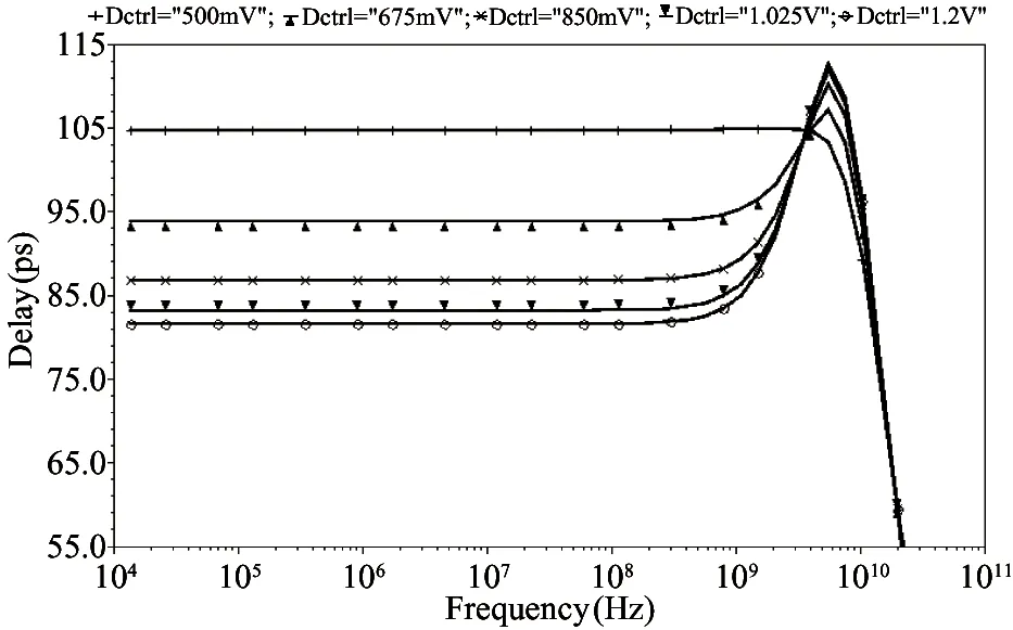

3 Experimental results

4 Conclusion
猜你喜歡
廈門大學學報(哲學社會科學版)(2022年5期)2022-10-11 01:22:46
中國外匯(2019年17期)2019-11-16 09:31:12
現代裝飾(2019年10期)2019-10-17 02:03:44
中國外匯(2019年21期)2019-05-21 03:04:24
銀行家(2017年1期)2017-02-15 20:27:53
華人時刊(2017年19期)2017-02-03 02:51:36
中國老區建設(2016年3期)2017-01-15 13:53:21
僑園(2016年5期)2016-12-01 05:23:41
創新作文(小學版)(2016年20期)2016-08-22 09:11:22
上海國資(2015年8期)2015-12-23 01:47:31
 High Technology Letters2017年3期
- High Technology Letters的其它文章
- A leveling mechanism for the platform based on booms-constraint control of aerial vehicle①
- Characterizing big data analytics workloads on POWER8 SMT processors①
- The rough representation and measurement of quotient structure in algebraic quotient space model①
- Quantitative analysis of the performance of vector tracking algorithms①
- ZnO whiskers growth on the surface of Sn9Zn/Cu solder joints in concentrator silicon solar cells solder layer①
- Structure design of gradient hard coatings on YG8 and their residual stress analysis by ANSYS①