A 90?mixed-mode twisted nematic liquid-crystal-on-silicon with an insulating protrusion structure?
2021-06-26 03:29:36WenJuanLi李文娟YuQiangGuo郭玉強(qiáng)ChiZhang張弛HongMeiMa馬紅梅andYuBaoSun孫玉寶
Chinese Physics B 2021年6期
Wen-Juan Li(李文娟) Yu-Qiang Guo(郭玉強(qiáng)) Chi Zhang(張弛)Hong-Mei Ma(馬紅梅) and Yu-Bao Sun(孫玉寶)
1School of Electronic and Information Engineering,Hebei University of Technology,Tianjin 300401,China
2Department of Applied Physics,Hebei University of Technology,Tianjin 300401,China
3School of Instrumentation Science and Opto-electronics Engineering,Beihang University,Beijing 100191,China
Keywords: liquid-crystal-on-silicon,mixed-mode twisted nematic,fringing field effect,reflectance
1. Introduction
Nowadays,with the advent of 5G,[1]the intelligent wearable devices have been put forward, especially the next generation wearable devices: near-eye display in virtual reality(VR). Against this backdrop, it requires fast response speed and high resolution to realize super image quality.[2–4]Organic light emission display(OLED)was thought to be suitable for the screen of virtual reality head mount displays (VR-HMD)because of its fast response speed.[5]However, it is difficult to obtain high resolution. The deposition of the OLED RGB emission layer was done through a metal mask. Small pixel pitch is required to obtain high-definition images, so the reducing pixel size is conceptually a straightforward way to increase the resolution of display.[6–8]Liquid-crystal-on-silicon(LCoS)[9]has been used extensively in near-eye virtual reality displays in micro-displays.[6,10–18]High resolution LCoS can be fabricated based on the high electron mobility of crystalline silicon.[19]However, with the decreasing of pixel size in the high-resolution LCoS device,the fringe field-effect between adjacent pixels becomes obvious.[20–26]It is difficult to drive one individual pixel because of the electric field leakage and penetration of the LC elastic force into adjacent pixels.[27]The fringing field can influence the liquid crystal distribution in the adjacent pixels,and ultimately degrade the optical performance severely.[28,29]To overcome this problem, several approaches have been pointed out,such as Eq.(1)employing weak fringing field effect liquid crystal mode: mixed-mode twist nematic (MTN).[30–32]The light propagation in MTNLCoS combines the polarization rotation and birefringence effects,[33,34]so it not only shows the advantage of weak fringing field effect,but also shows high reflectance and low operation voltage. Equation (2) optimizing the structure of LCoS cell: the low dielectric constant polymer wall has been proposed to isolate the pixels in the LC cell,[34]and the dielectric shield wall structure and lattice-shaped dielectric walls have been proposed[27,35]as well.These structures can significantly reduce the fringing field effect of the LCoS device.
In this paper, we will propose a protrusion located between the adjacent pixels in the high-resolution LCoS device,analyze the effect of the protrusion in the voltage-on pixel and the adjacent voltage-off pixels in 90?-MTN mode,and investigate the fringe field effect.The invalid pixel region is proposed to define the fringe field effect. The results show that the protrusion between the adjacent pixels can significantly reduce the fringe field effect in LCoS devices.
2. Device structure and theory
Figure 1 depicts the device configuration of protrusion located between the adjacent pixels in the high-resolution LCoS.In such a configuration, a polarizing beam splitter (PBS) is set in front of the top glass and its polarizer’s axis is at 0?,indium-tim-oxide(ITO)as the common electrode is coated on the top glass substrate, and aluminum electrodes as the pixel electrodes are coated on the bottom silicone substrate. LC is sandwiched between the two substrates, and its twist angle is 90?(?20?to 70?). As evident from Fig.1,dis the LC layer’s thickness of the LCoS cell,lis the pixel size, andw1is the gap of pixels,w2andhare the width and the height of the protrusion,respectively.
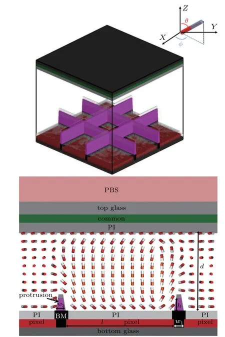
Fig.1. Configuration of LCoS with protrusion located between the adjacent pixels.
In simulation, the extended Jones matrix method and Frank’s continuum theory have been used to calculate the voltage-dependent reflectance.[32,36]For the off-state, the optical transmittance of the twisted LC layer can be described as[32]

In the simulation,the pretilt angle is 2?,the pixel’s width isl=10 μm, and its gap is varied from 0.5 μm to 0.8 μm.The LC material has ?ε=5.3, ?n=0.096 (λ=550 nm),d=2.5μm,K11=10.87 pN,K22=9.5 pN,K33=15.37 pN.In order to obtain the high reflection and reduce the fringe field effect,the width of the protrusion(w2)is varied from 0.5μm to 0.9μm,the height of the protrusion(h)is varied from 0.3μm to 0.7μm,and the dielectric constant is 4.0.
3. Results and discussion
From Fig. 2, there are two cases for the influence of the adjacent pixels: (a) the dark invalid pixel region (the region withR <0.1Rmaxin bright pixel), and (b) the bright invalid pixel region(R >0.1Rmaxin black pixel). In the sudoku pixels, the middle one is driven by the operate voltage to obtain the dark pixel (voltage-on pixel), and other eight pixels are named as the bright pixels (voltage-off pixels). The dark region extends into the adjacent bright pixel, we call the dark region in white pixel as the dark invalid pixel region,L1bandL2bare theX-direction widths of the dark invalid pixel region on the left and right sides of the voltage-on pixel. The totalX-direction width of the dark invalid pixel region on both sides (Lb=L1b+L2b) is shown in Fig. 2(a). On the other hand, the bright region in the dark(voltage-on)pixel is called as the bright invalid pixel region,L1wandL2ware theX-direction widths of the bright invalid pixel region on the two sides. The totalX-direction width of the bright invalid pixel region on both sides(Lw=L1w+L2w) is shown in Fig. 2(b).IfLw>0, the dark state shows a serious light-leakage, this case can reduce the contrast ratio,so it needs to be eliminated at the first. When the height of the protrusion is small (less than 0.7μm),there is only the inherent elasticity of the liquid crystal, the protrusion has a little effect on the LC alignment between adjacent pixels. When the height of the protrusion is larger than 0.7μm in our simulation,most of the liquid crystal molecules are on two sides of the protrusion. The LC alignment and surface forces at the edges of the protrusion are the same as those on the substrates surface. The protrusion prevents the liquid crystal molecules from twisting in response to an electric field. When the pixel turns black with voltage applied,the region will appear white. From Fig.2(b),the too large height of the protrusion leads to the bright invalid pixel region,so the height of the protrusion is chosen to be less than 0.7 μm forLw=0, the total invalid pixel region widthLton theX-direction is written as
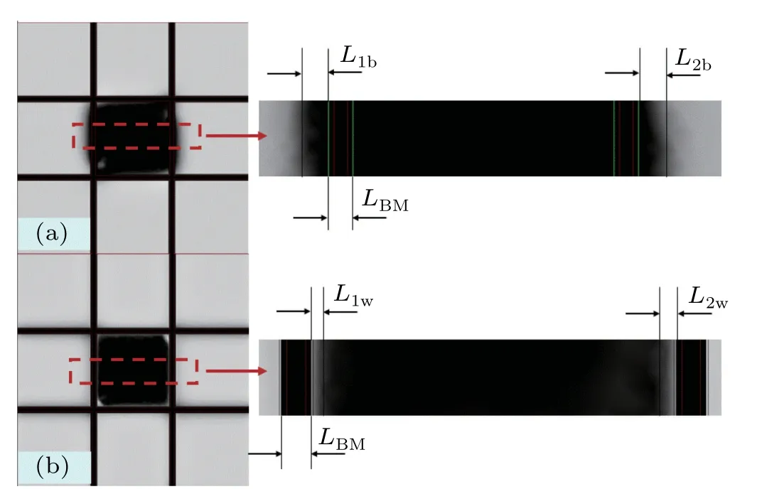
Fig. 2. The X-direction width of the invalid pixel region in normal-white mode. (a)The dark invalid pixel region for the protrusion with h=0.5μm and w2=0.5μm. (b)The bright invalid pixel region for the protrusion with h=2.0μm and w2=0.5μm.

To evaluate the electro-optic characteristics of 90?-MTN LCoS with a protrusion located between the adjacent pixels,we simulate the voltage-dependent reflectance of the cell,which has the protrusion with different heights from 0.3 μm to 0.7 μm and different widths from 0.5 μm to 0.9 μm. As shown in Fig.3,the reflectance is influenced by the height and width of the protrusion,but its change is within 1.3%,and it is small enough to be regarded as the dark state when the voltage reaches 5 V.The off-state voltage(Voff)is 0 V and the on-state voltage (Von) is 5 V. We simulate theX-direction reflectance(X–R)curves atVon=5 V to compare the invalid pixel regions of the cell with different heights and widths.

Fig.4. Simulated X–R curves for different protrusion heights from 0.3μm to 0.7μm and(a)w2=0.5μm,(b)w2=0.6μm,(c)w2=0.7μm,(d)w2=0.8μm,(e)w2=0.9μm,(f)compare with no protrusion.

Fig. 3. Simulated V–R curves of the protrusion with different heights from 0.3μm to 0.7μm for(a)w2 =0.5μm,(b)w2 =0.6μm,(c)w2 =0.7μm,(d)w2=0.8μm,(e)w2=0.9μm,and(f)compared with no-protrusion.
Figure 4 depicts theX–Rcurves for the protrusion with different heights from 0.3μm to 0.7μm and different widths from 0.5μm to 0.9μm.To avoid reducing the display area,the protrusion’s width(the rectangle with solid line and gray black color) is not larger than the width of the black matrix (BM)(the rectangle with dashed line,0.9μm),where the protrusion width is varied from 0.5 μm (the pixel gap) to 0.9 μm (the BM width). As no protrusion is used, the dark invalid pixel region in the adjacent bright(voltage-off)pixels is obvious,Lbis decreased as the protrusion’s height increases from 0.3μm to 0.7 μm for all above widths. Moreover, the reflectance at the edges of the protrusion in the dark pixel (voltage-off) increases with the increasing height of the protrusion because of the surface anchoring of the alignment layer on the protrusion and the inherent elasticity of the LC layer,as a result,Lwis not zero. For avoiding the bright invalid pixel region,the width of the protrusion is smaller than the BM’s width,the height of the protrusion is also smaller than a critical value.
From Table 1,the total invalid pixel region width for the cell without protrusion is 3.345 μm, and it decreases as the protrusion height increases from 0.3μm to 0.7μm for the different protrusion widths (0.5 μm, 0.6 μm, 0.7 μm, 0.8 μm,0.9μm).

Table 1. The Lt for the SiO2 protrusion with different heights and different widths.
Based onLw= 0, whenw2=0.5 μm, the height is less than 0.7μm,Ltis decreased from 12.9%to 31.5%compared with that without protrusion as the protrusion height increases from 0.3 μm to 0.7 μm, andLw>0 when the protrusion height is larger than 0.7 μm. TheLtof the protrusion withh=0.6 μm andw2=0.5 μm is the smallest, 31.5% smaller than that without protrusion. Whenw2=0.6μm,the protrusion height needs to be less than 0.6μm, andLtis decreased from 20.9%to 23.0%as the protrusion height increases from 0.3μm to 0.5μm. Whenw2=0.7μm,the protrusion height needs to be less than 0.6μm,andLtis decreased from 20.9%to 31.5% as the protrusion height increases from 0.3 μm to 0.5μm. Whenw2=0.8μm,the protrusion height needs to be less than 0.5 μm, andLtis decreased from 23.0% to 31.5%as the protrusion height increases from 0.3 μm to 0.4 μm.Whenw2=0.9μm,theLtwith the protrusion ofh=0.3μm is 23.0%smaller than that without protrusion. Hence,three sets of(h,w2)with the smallestLtare(h=0.4μm,w2=0.8μm),(h=0.5μm,w2=0.7μm),and(h=0.6μm,w2=0.5μm),the total width of the invalid pixel region is reduced by 31.5%compared with that of the cell without protrusion.[38]
The comparison of the liquid crystal distribution for the cells without and with protrusion(h=0.6μmw2=0.5μm)has been made,as illustrated in Fig.5. When there is no wall protrusion between the adjacent pixels, the pixel shows the rounded edges at the left and right sides, so the dark invalid region is large. When the protrusion with 0.5 μm width and 0.6μm height is located between the adjacent pixels,the dark invalid region is reduced more,and few smaller bright invalid regions exist at the corners of the black pixels(Lw≈0).
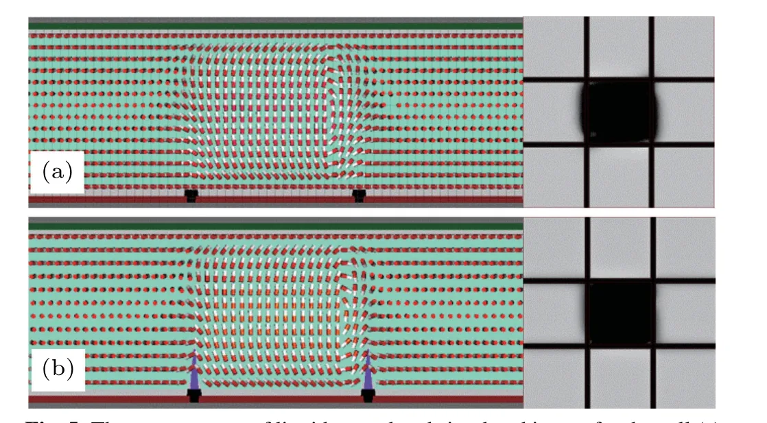
Fig.5. The arrangement of liquid crystal and simulated image for the cell(a)without protrusion,and(b)with protrusion(h=0.6μm w2=0.5μm).
4. Conclusion
The total invalid pixel region width of an MTN-LCoS with different protrusion’s widths and heights is calculated.The results indicate that the total invalid pixel region width can be reduced by 31.5%with the suitable protrusion’s width and height, so the contrast ratio can be improved. The protrusion can be fabricated by the traditional photoresist development method or nanoimprinting method,[35]which matches the photolithography process. The material can be chosen as the organic material,such as photoresist,which has good softness and is not fragile. These results have an important influence on improving the electro-optic characteristics of LCoS.

- Chinese Physics B的其它文章
- Coarse-grained simulations on interactions between spectrins and phase-separated lipid bilayers?
- Constraints on the kinetic energy of type-Ic supernova explosion from young PSR J1906+0746 in a double neutron star candidate?
- Computational model investigating the effect of magnetic field on neural–astrocyte microcircuit?
- Gas sensor using gold doped copper oxide nanostructured thin films as modified cladding fiber
- Exact explicit solitary wave and periodic wave solutions and their dynamical behaviors for the Schamel–Korteweg–de Vries equation?
- Suppression of ferroresonance using passive memristor emulator