Anisotropic thermoelectric transport properties in polycrystalline SnSe2?
2021-06-26 03:04:22CaiyunLi李彩云WenkeHe何文科DongyangWang王東洋andLiDongZhao趙立東
Chinese Physics B 2021年6期
Caiyun Li(李彩云), Wenke He(何文科), Dongyang Wang(王東洋), and Li-Dong Zhao(趙立東)
School of Materials Science and Engineering,Beihang University,Beijing 100191,China
Keywords: thermoelectric,SnSe2,anisotropic structure,Cl-doping
1. Introduction
Thermoelectric material, as the main body of device for reversible conversion between waste heat and electricity, can effectively alleviate the shortage of traditional primary energy and improve the situation of environmental degradation.[1,2]The dimensionless figure of merit (ZT) can be used to assess the conversion ability of thermoelectric materials for practical production and application,defined asZT=S2σT/κtot,whereS,σ,κtot, andTare the Seebeck coefficient, electrical conductivity,total thermal conductivity,and absolute temperature,respectively.[3–5]In recent years, a series of new theories and advanced material fabrication technologies have been developed to optimize the thermoelectric properties,[6–16]such as raising power factor(PF=S2σ)through employing the band structure engineering[7,8,17]or lowering thermal conductivity by adopting defect engineering.[11,18–23]In addition,a certain material with low intrinsic thermal conductivity is explored to evade election–phonon coupling effectively.[14,24–27]
As a compound consisting of the same elements as SnSe,SnSe2has attracted much attention owing to not only its features of nontoxicity, non-pollution, earth-abundant, and low cost,[28]but also its natural layered structure leading to a low thermal conductivity,[29]making it become a competitive material in the field of thermoelectricity. Moreover, the firstprinciples calculations forecasted that SnSe2is able to reach a promisingZTvalue of~2.95 in n-type SnSe2crystals when the carrier concentration (n) is raised to~1020cm?3at 800 K.[30]SnSe2is crystallized in a typical structure of CdI2(Figs. 1(a)–1(c)), and Se accumulates in a densely arranged hexagonal form while Sn is in the octahedral interstice surrounded by six Se atoms.[31]Similar to many layered compounds (Bi2Se3, Bi2Te3, etc.),[32]n-type polycrystalline SnSe2exhibits anisotropic thermoelectric properties along thea-axis andc-axis,[33]the weaker van der Waals chemical bonding between the layers makes the acoustic phonon mode along thec-axis softer than that along thea-axis, and results in a much lower thermal conductivity along the interlayer direction(c-axis).[34]When sintering the polycrystalline SnSe2samples,the layered structures are inclined to distribute along the sintering pressure direction. Therefore,superiorZTvalues are generally obtained along the pressuring direction owing to the much lower thermal conductivity.[18,30,33]
Among the diverse approaches for optimizing SnSe2,the substitution of halogen atoms in Se sites is proved to be a convenient and highly effective strategy to increase the carrier concentration, and thus improves its electrical performance.[29,33,35–37]Shuet al. reported a highZTof~0.56 at 773 K in n-type polycrystalline SnSe2as the doping concentration of Cl reaches to~6%.[36]Further, Liuet al. built an imbedded Ag+bridge in the layers of SnSe2and harvested a record-breakingZTof~1.03.[18]However, the excessive increment of carrier concentration in the SnSe2matrix will inevitably result in a higher thermal conductivity from the electron contribution. In this case,we first introduce SnSe phase into SnSe2to reduce the lattice thermal conductivity because of the inter-phase scattering between SnSe2matrix and the second phases.[38–41]Subsequently, we select Cl dopant to optimize the carrier concentration and improve the electrical performance. Meanwhile, the anisotropic thermoelectric transport properties are investigated and analyzed in SnSe2-based samples. We find a~3 times lower thermal conductivity along the direction parallel to the spark plasma sintering(SPS) pressure (‖P), and a~2 times higherPFalong the direction perpendicular to the SPS pressure (⊥P) in SnSe2-based samples. As a result, comprehensive consideration on the electrical properties and thermal conductivity,a higherZTis attained along the‖ Pdirection. Besides, the minimum thermal conductivity decreases from~0.57 W·m?1·K?1to~0.39 W·m?1·K?1after introducing 2%SnSe along the‖Pdirection. Then, the maximumPFyields a sharp increase in SnSe2-2% SnSe after 5% Cl doping, which increases from~1.70μW·cm?1·K?2to~9.76μW·cm?1·K?2along the⊥Pdirection. In the end, theZTvalue is improved to as high as~0.6 after the two-step optimization along the‖Pdirection.All above optimizing processes are summarized in Fig.2.
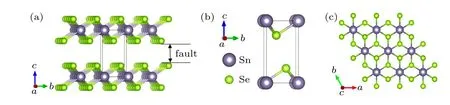
Fig.1. Crystal structure of SnSe2: (a)crystal structure along the a-axis;(b)the unit cell;(c)crystal structure along the c-axis.
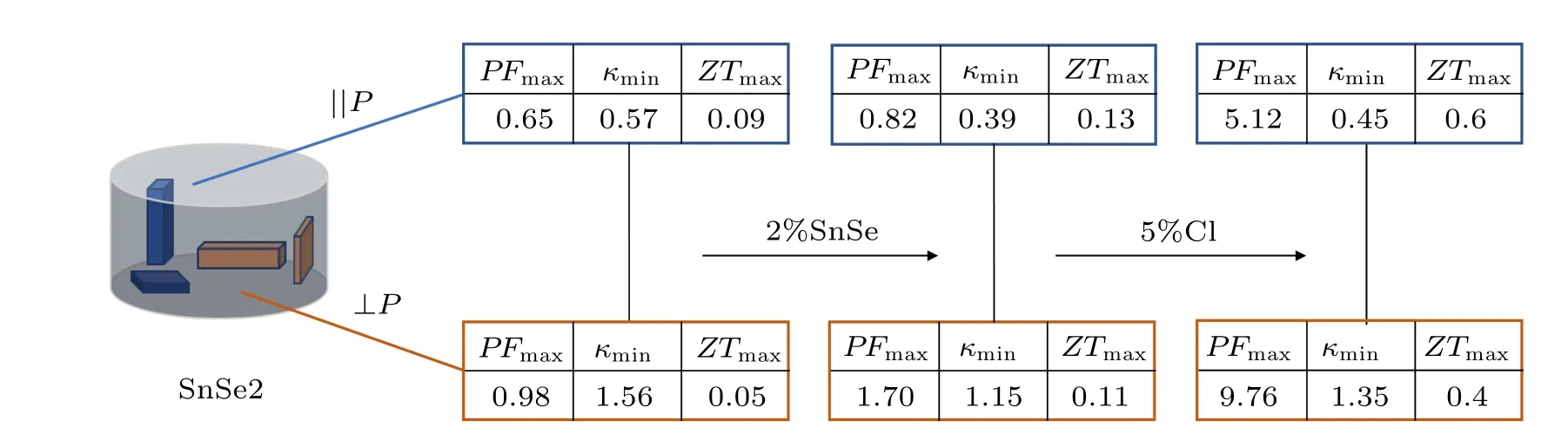
Fig. 2. A two-step optimization process for SnSe2 along the ‖P and ⊥P directions. The units of PFmax and κmin are μW·cm?1·K?2 and W·m?1·K?1,respectively.
2. Results and discussion
The powder XRD patterns of the SnSe2-x% SnSe composites (x=0, 1, 2, 3) are shown in Fig. 3(a). It is found that the diffraction peaks are well consistent with the simulated pattern (PDF# 01-089-2939). The lattice parameters do not change after adding 1% SnSe whatever the addition of SnSe content, which indicates the presence of SnSe phase(Fig.3(b)).From the band gap measurement results(Figs.3(c)and 3(d)), the band gap slightly decreases after adding SnSe into SnSe2,which is due to the relative low band gap of SnSe.
The electrical conductivities of SnSe2-x% SnSe samples along the two directions (‖ Pand⊥P) are measured in the temperature range from 300 K to 773 K(Figs.4(a)and 4(b)).The electrical conductivity is very low at room temperature and then increases as the temperature rises, which is a typical temperature-dependent intrinsic semiconductor feature.The electrical conductivity depends weakly on the temperature from 300 K to 600 K.At high temperatures,the electrical conductivity after adding SnSe is higher than that of pristine SnSe2,which may come from that the reduced band gap from introducing SnSe is more conducive to thermal excitation as the temperature rises. This behavior is more striking along the⊥Pdirection in this layered compound. It is obvious that the electrical conductivity along the⊥Pdirection is superior to that along the‖Pdirection,which indicates an outstanding⊥Pdirection(can be considered as the in-plane direction in crystals)electrical transport property in SnSe2. Besides, the Seebeck coefficients of all samples are relatively large and maintain within the range of~?400μV·K?1to?600μV·K?1at the whole working temperature(Figs.4(c)and 4(d)).As a consequence,the power factors after introducing SnSe are higher than that of pristine SnSe2, especially in the polycrystalline samples along the⊥Pdirection(Figs.4(e)–4(f)). A maximum power factor of~1.7 μW·cm?1·K?2at 773 K is attained in SnSe2along the⊥Pdirection, and is twice of that along the‖Pdirection, which is ascribed to the excellent in-plane carrier mobility in SnSe2.
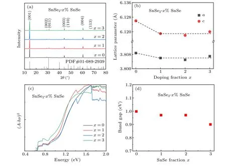
Fig.3. (a)XRD patterns;(b)the lattice parameters;(c)UV–vis absorption spectra,and(d)band gaps for SnSe2-x%SnSe.
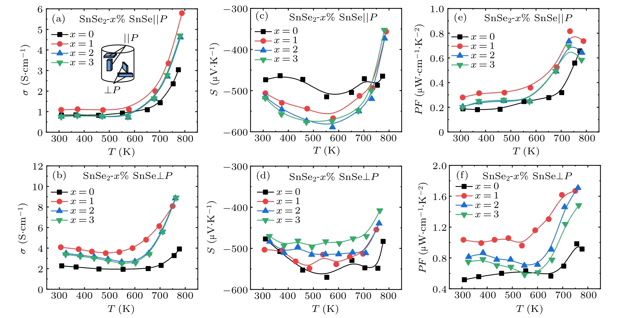
Fig. 4. Temperature dependence of electrical transport properties along the ‖P and ⊥P directions for SnSe2-2% SnSe: (a)–(b) electrical conductivities;(c)–(d)Seebeck coefficients;(e)–(f)power factors.
To further investigate the difference in electrical properties after adding SnSe and along the two directions in SnSe2, the Hall measurements are conducted. Since SnSe is a p-type phase in SnSe2, the room-temperature (RT) carrier concentration decreases from~1.17×1018cm?3to~5.62×1017cm?3, but a high carrier mobility (μ) is obtained from~1.82 cm2·V?1·s?1to~8.16 cm2·V?1·s?1and~10.57 cm2·V?1·s?1to~38.05 cm2·V?1·s?1along the‖Pand⊥Pdirections,respectively(Figs.5(a)and 5(b)). The carrier mobilities along these two directions also show a significant distinction,the values along the⊥Pdirection are~5–10 times higher than those along the‖Pdirection. Based on the single parabolic band model,[42]we have calculated the carrier mobility as a function of carrier concentration(Fig.5(c)). All the experimental data are under the simulated curve, which is attributed to the more complex scattering mechanism in polycrystalline samples, such as grain boundary, precipitated phase, etc.[39,43]Moreover, on the basis of the single band model,the Seebeck coefficient can be obtained as[44,45]
wherekBrepresents the Boltzmann constant,hrepresents the Planck constant, andm?represents the density of state effective mass. The Pisarenko line shows that the effective masses along the two directions are almost unchanged after increasing the SnSe concentration,indicating a single band transport feature at low carrier concentration in SnSe2(Fig.5(d)).
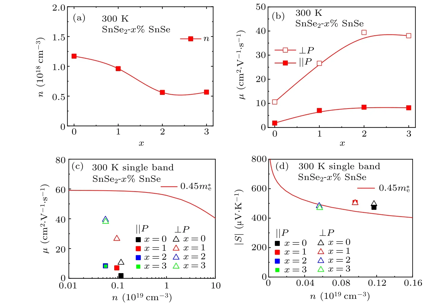
Fig. 5. (a) Carrier concentration; (b) carrier mobility; (c) carrier mobility, and (d) Seebeck coefficient as a function of carrier concentration along the‖P and ⊥P directions for SnSe2-x%SnSe.
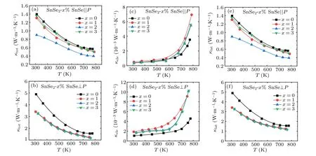
Fig. 6. The temperature dependence of thermal conductivity along the ‖P and ⊥P directions for SnSe2-2% SnSe: (a)–(b) total thermal conductivity;(c)–(d)electronic thermal conductivity;(e)–(f)lattice thermal conductivity.
The total thermal conductivity(κtot)for all samples continuously decreases with elevating temperature(Figs.6(a)and 6(b)). It can be seen that theκtotwith SnSe phase along the‖Pand⊥Pdirections are lower than those of pristine SnSe2.Besides, theκtotalong the‖Pdirection is much lower than that along the⊥Pdirection. Theκtotmainly comes from the contributions of electronic thermal conductivity(κele)and lattice thermal conductivity (κlat). Theκeleis calculated byκele=LσT,whereLis the Lorentz constant,theκeleincreases as temperature rises,which is mainly due to the increased electrical conductivity at high temperatures (Figs. 6(c) and 6(d)).The lattice thermal conductivity(κlat)can be obtained by subtractingκelefromκtot,namely,κlat=κtot?κele. Interestingly,the overallκlatalong the‖ Pdirection is~3 times lower than that along the⊥Pdirection (Figs. 6(e) and 6(f)). Moreover,a lowκlatof~0.39 W·m?1·K?1is obtained at 773 K in SnSe2-2%SnSe sample along the‖Pdirection while theκlatin the pristine SnSe2sample is~0.56 W·m?1·K?1,implying a strong inter-phase scattering after introducing 2%SnSe.
In order to further explore the decline of the lattice thermal conductivity, we calculate the Gr¨uneisen constant (γ) of these two samples along the‖Pdirection,[46,47]as shown in Table 1.Theγof these two samples are~3.03 and~2.95,respectively,which indicates that the sample with 2%SnSe has a stronger anharmonicity.
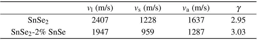
Table 1. The longitude sound velocity(vl),shear sound velocity(vs),average sound velocity(va),and Gr¨uneisen parameters(γ)of SnSe2 and SnSe2-2%SnSe.
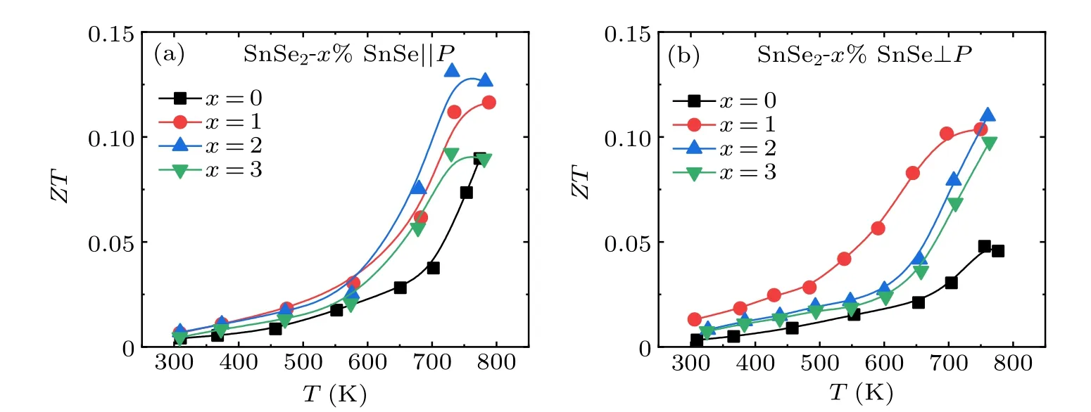
Fig.7. Temperature dependent ZT values along the(a)‖P and(b)⊥P directions for SnSe2-2%SnSe.
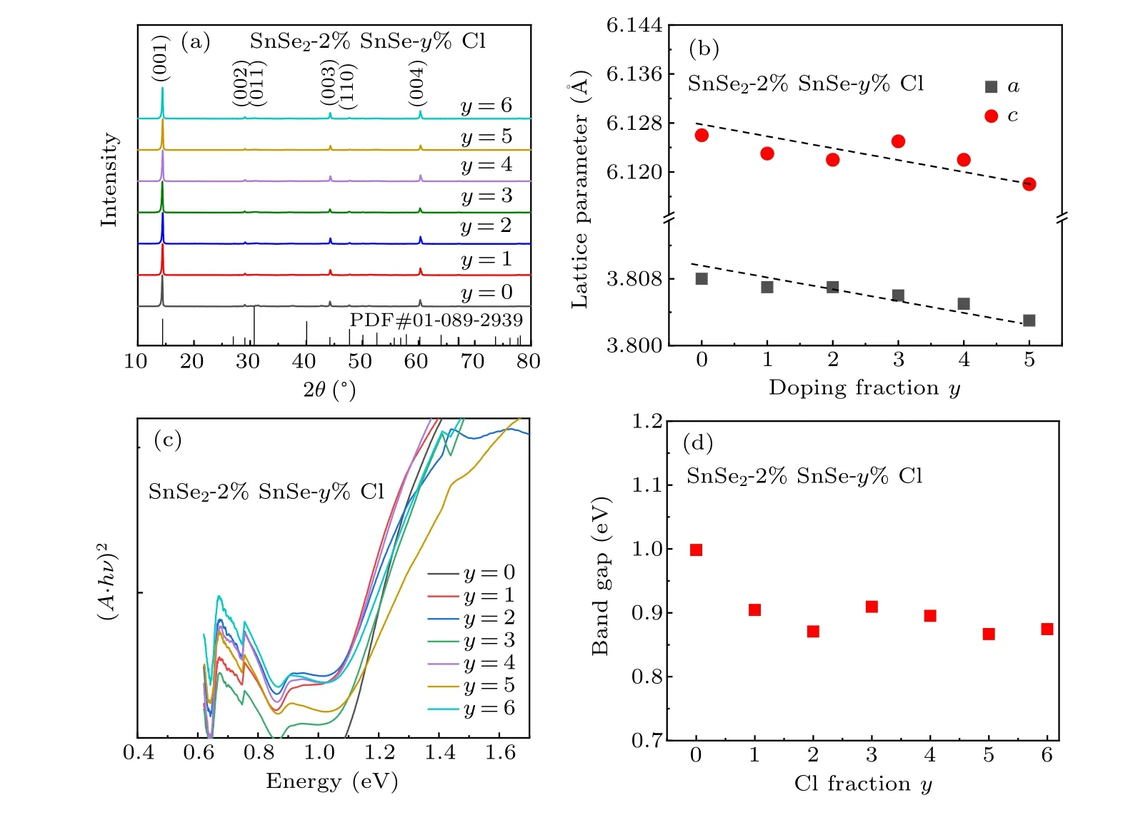
Fig.8. (a)XRD patterns;(b)lattice parameters;(c)UV–vis absorption spectra,and(d)band gap for SnSe2-2%SnSe-y%Cl.
Compared with the excellent electrical transport properties along the⊥Pdirection,the contribution from thermal conductivity along the‖Pdirection to finalZTs is more strikingly, especially when introducing SnSe phase with intrinsically lowκlat. Therefore,combining the electrical and thermal properties along the two directions, relatively higherZTs are achieved along the‖Pdirection(Figs.7(a)and 7(b)). TheZTvalue along the‖Pdirection approaches to as high as~0.13 at 773 K for SnSe2-2%SnSe while is only~0.09 for SnSe2.
Based on the obtained low thermal conductivity and highZTin SnSe2with 2% SnSe, we further improve the electrical transport properties through halogen element doping. The XRD data of all samples with Cl doping are shown in Fig.8(a).It is obvious that all the diffraction peaks agree well with the simulated pattern (PDF# 01-089-2939) (SnSe2-2% SnSe-y%Cl,y=0, 1, 2, 3, 4, 5, 6). Figure 8(b) shows that the lattice parameter gradually decreases with increasing Cl content, it proves that Cl is doped into SnSe2matrix as Cl has a smaller atomic radius than Se. The decrement of band gap from~1.0 eV to~0.83 eV is likely related to the introduction of impurity energy levels after Cl doping (Figs. 8(c) and 8(d)).
After Cl doping, the carrier concentration is optimized,leading to a huge increment of electrical conductivity (σ) in SnSe2-2% SnSe samples. At room temperature, theσincreases from~4 S·cm?1to~78 S·cm?1and from~9 S·cm?1to~208 S·cm?1along the‖Pand⊥Pdirections after 5%Cl doping, respectively (Figs. 9(a) and 9(b)). This striking difference mainly derives from the unique layered structure of SnSe2as mentioned above. The Seebeck coefficient decreases after increasing carrier concentration along the two directions (Figs. 9(c) and 9(d)). Besides, it can be seen that thePFreaches to as high as~5.12 μW·cm?1·K?2and~9.76 μW·cm?1·K?2after 5% Cl doping along the‖Pand⊥Pdirections, respectively (Figs. 9(e) and 9(f)), which is an prominent enhancement compared to the undoped samples.
To further investigate the dramatic increase in theσ, thenandμat room-temperature are measured. As Fig.10(a)depicts, thenis largely enhanced from~5.6×1017cm?3to~6.2×1019cm?3after Cl doping, which benefits from the fact that Cl is an effective electron donor.[35]It is worth noting that theμincreases with rising the doping concentration from 1%to 5%(Fig.10(b)),which may be due to the microregulation of Cl on SnSe2and SnSe phases.[36]In other word,Cl replaces Se not only in SnSe2but also in SnSe, making the SnSe phase be changed from intrinsic p-type to n-type,therefore, the n–p phase in SnSe2convert to n–n phase thus reducing the energy barrier between SnSe2and SnSe, which makes the carriers facilely migrate. As a consequence, theμincreases up to~12 cm2·V?1·s?1after 5% Cl doping along the‖Pdirection. Based on the single parabolic model,[42]experimental data locate under the simulated relationship curve ofμwith increasednobviously (Fig. 10(c)), which is attributed to the dominance of grain boundary scattering in polycrystalline SnSe2at low temperatures.[48]Based on the Pisarenko relationship,[38,44]it is found that the effective mass increases after Cl doping(Fig.10(d)),which implies a multiple band transport behavior in SnSe2as the carrier concentration rises.[35]
Fig. 9. The temperature dependence of electrical transport properties along the ‖P and ⊥P directions for SnSe2-2% SnSe-y% Cl samples:(a)–(b)electrical conductivities;(c)–(d)Seebeck coefficients;(e)–(f)power factors.
It is found that the wholeκtotafter Cl doping are slightly higher compared to those of the undoped 2% SnSe samples, which are in the range of~0.45 W·m?1·K?1to~1.35 W·m?1·K?1at 773 K (Figs. 11(a) and 11(b)). Besides, theκeleincreases rapidly with increasing the doping content owing to the contribution from the increased carrier concentration (Figs. 11(c)and 11(d)). In the end, theκlatincreases slightly after Cl doping along the two directions,which may come from the reduced energy barrier between SnSe2and SnSe phases weakening the inter-phase scattering after Cl doping(Figs.11(e)and 11(f)).
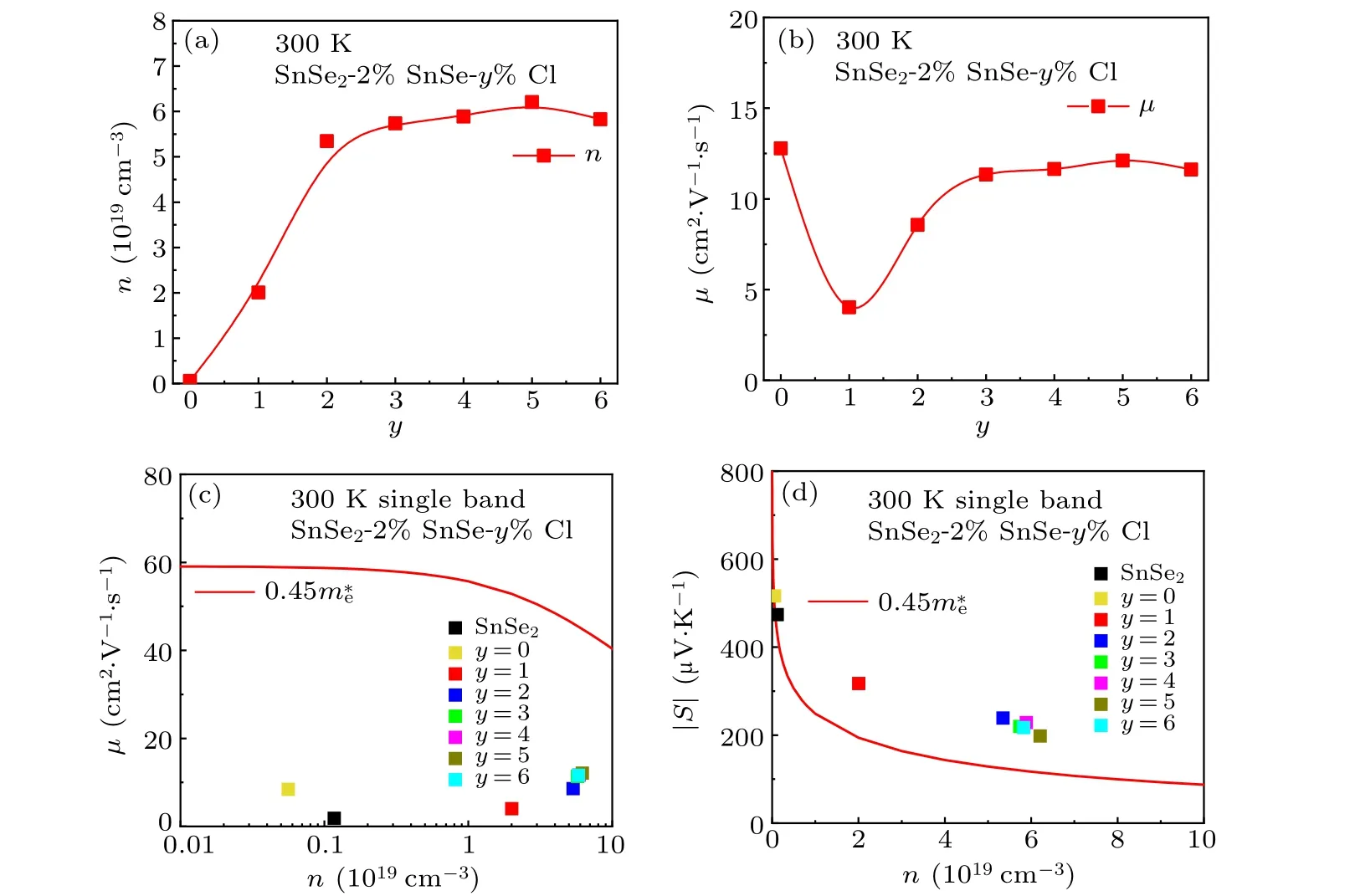
Fig.10. (a)Carrier concentration;(b)carrier mobility;(c)carrier mobility,and(d)Seebeck coefficient as function of carrier concentration for SnSe2-2%SnSe-y%Cl.
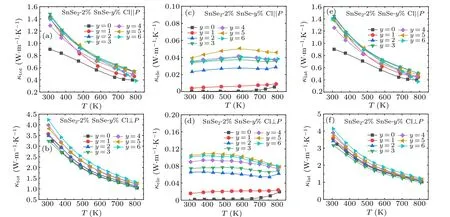
Fig. 11. The temperature dependence of thermal conductivities along the ‖P and ⊥P directions for SnSe2-2% SnSe-y% Cl: (a)–(b) total thermal conductivities;(c)–(d)electronic thermal conductivities;(e)–(f)lattice thermal conductivities.
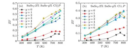
Fig.12. Temperature dependent ZT values along the(a)‖P and(b)⊥P directions for SnSe2-2%SnSe-y%Cl.
Through the comprehensive evaluation on the anisotropic electrical properties and thermal conductivity of SnSe2-2%SnSe with Cl doping, the samples show higherZTvalues along the‖Pdirection than the⊥Pdirection(Figs.12(a)and 12(b)). Finally,a maximumZTof~0.6 at 773 K is achieved in SnSe2-2%SnSe-5%Cl along the‖Pdirection, which is a great improvement compared toZTof~0.13 for the SnSe2-2%SnSe sample without Cl doping.
2.1. Conclusion
In summary, the thermoelectric performance of SnSe2is improved successfully by a two-step optimization strategy,namely,reducing the thermal conductivity by introducing SnSe and then increasing the power factor through Cl doping.Specifically, introducing SnSe phase can significantly reduce the lattice thermal conductivity in SnSe2due to the inter-phase scattering and strong anharmonicity,then Cl doping optimizes the carrier concentration thus improving the electrical properties. Meanwhile,we also estimate that the anisotropic thermoelectric properties along the‖Pand⊥Pdirections in SnSe2-based samples, and find a more prominent contribution from the thermal conductivity to the finalZTs along the‖Pdirection. Ultimately,a highZTof~0.6 along the‖Pdirection is achieved for SnSe2-2% SnSe-5% Cl sample at 773 K, which makes it a promising candidate for thermoelectric application.

- Chinese Physics B的其它文章
- Coarse-grained simulations on interactions between spectrins and phase-separated lipid bilayers?
- Constraints on the kinetic energy of type-Ic supernova explosion from young PSR J1906+0746 in a double neutron star candidate?
- Computational model investigating the effect of magnetic field on neural–astrocyte microcircuit?
- Gas sensor using gold doped copper oxide nanostructured thin films as modified cladding fiber
- Exact explicit solitary wave and periodic wave solutions and their dynamical behaviors for the Schamel–Korteweg–de Vries equation?
- Suppression of ferroresonance using passive memristor emulator