Terminal-optimized 700-V LDMOS with improved breakdown voltage and ESD robustness?
2021-06-26 03:30:12JieXu許杰NaiLongHe何乃龍HaiLianLiang梁海蓮SenZhang張森YuDeJiang姜玉德andXiaoFengGu顧曉峰
Chinese Physics B 2021年6期
Jie Xu(許杰) Nai-Long He(何乃龍) Hai-Lian Liang(梁海蓮)Sen Zhang(張森) Yu-De Jiang(姜玉德) and Xiao-Feng Gu(顧曉峰)
1Engineering Research Center of IoT Technology Applications(Ministry of Education),Department of Electronic Engineering,Jiangnan University,Wuxi 214122,China
2Technology Development Department,CSMC Technologies Corporation,Wuxi 214061,China
Keywords: lateral double-diffused MOSFET (LDMOS), terminal-optimization, breakdown voltage, electrostatic discharge
1. Introduction
The lateral double-diffused metal–oxide semiconductor(LDMOS) has wide applications in power integrated circuits due to its high breakdown voltage (BV) and high current capability.[1–3]The LDMOS with interdigitated structure is usually adopted for high current capability, benefiting from the increased device width. However,theBVof the interdigitated LDMOS is reduced due to the curvature effect and high electric field in the terminal region. To suppress the curvature effect,Komatsuet al.proposed a novel LDMOS by increasing the curvature radius in the terminal region,[4]but its manufacturing cost increases with device size increasing. To reduce the electric field in the terminal region, Leeet al.optimized the LDMOS by inserting P-type rings around the source fingertip region,[5]but theBVcould not be improved remarkably by this method. On the other hand,the electrostatic discharge(ESD) performance of LDMOS is also very important for its practical applications.[6–8]With an ultrahigh operating voltage,the ESD robustness of LDMOS in high voltage(HV)circuit is quite weak,which is usually improved by enlarging the device width at the expense of increasing the manufacturing cost. Therefore,LDMOS needs to be further optimized by using more economical methods.
In this paper, a terminal-optimized triple RESURF LDMOS (TOTR-LDMOS) is proposed to improve theBVand ESD robustness without consuming additional chip area. Both traditional LDMOS and TOTR-LDMOS are fabricated, and their physical mechanisms are investigated by direct current(DC) tests, transmission line pulse (TLP) tests, and technology computer-aided design (TCAD) simulations. The results demonstrate that the TOTR-LDMOS with a higherBVand a stronger ESD robustness is a promising power device.
2. Device structure and mechanism
The schematic top view and internal structure of the traditional triple RESURF LDMOS is shown in Fig.1(a). It consists of active regions as the main working area and terminal regions as the bridge to connect two active areas.[9]TheBVof traditional LDMOS is mainly restricted by the curvature effect and high electric field in terminal regions. In order to increase theBV, the device structure is optimized by cutting the N-drift region in the terminal region and filling the area with a P-region, and the doping concentration of the P-layer falls in between the concentrations of P-substrate and Deep Pwell. The structure of the proposed TOTR-LDMOS is shown in Fig.1(b).
The cross-section structure of the active region in the TOTR-LDMOS along theAA'C'Cplane (marked in Fig. 1)is the same as that in the traditional LDMOS as shown in Fig.2(a).When the device is in the on-state,the heavily doped N-top layer provides a low-resistance path for electrons,leading to a lowRon,sp. When the device is biased in the off-state,the P-buried layer is completely exhausted by the upper N-top layer and the bottom N-drift region.
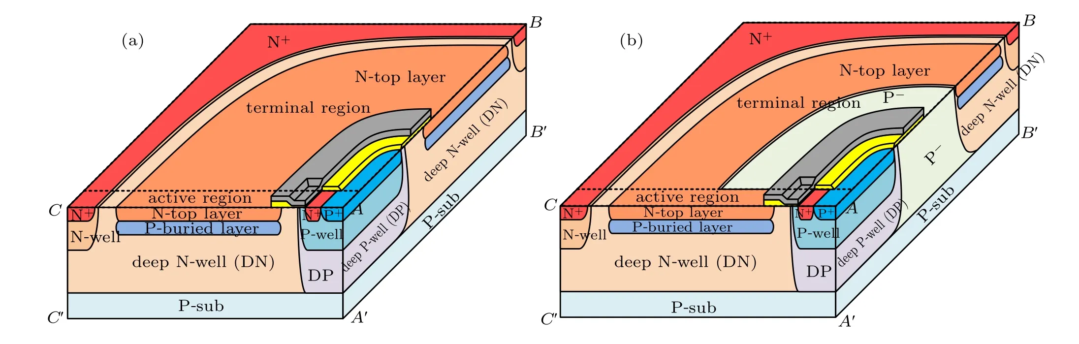
Fig.1. Schematic top view and internal structure of(a)traditional LDMOS and(b)TOTR-LDMOS.
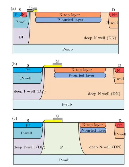
Fig.2. Cross-section structures when cutting along(a)AA'C'C surface and(b)AA'B'B surface of traditional LDMOS,and along(c)AA'B'B surface of TOTR-LDMOS.
The cross-section structures along theAA'B'Bplane of the terminal region in the traditional LDMOS and TOTR-LDMOS are shown in Figs.2(b)and 2(c),respectively.Comparing with the traditional LDMOS,a wide depletion region is formed in the TOTR-LDMOS by deep N-well and P–when the device is in the off-state. As a result, the electric field between the Pand deep N-well is weaker, resulting in a higherBV. On the other hand,the introduced P-region increases the curvature radius of PN junction in the terminal region,suppressing the curvature effect in the terminal region. As a result,the premature breakdown caused by current over-crowding in the terminal region is avoided. Besides,the weaker electric field reduces the impact ionization rate,avoiding thermal breakdown caused by the intense movement of charge carriers and further contributing to a higher second failure current(It2)of the device.
3. Results and discussion
3.1. Breakdown voltage
In order to verify the superiority of the TOTR-LDMOS,the experimental device as well as the traditional LDMOS is fabricated in a 0.25-μm bipolar-CMOS-DMOS(BCD)process and measured by Keysight B1505A.The process flow chart of the TOTR-LDMOS is summarized in Fig.3. Comparing with the traditional LDMOS, an extra layer P-well square is obtained by driving-in array of small deep P-well squares,without needing extra mask. The relevant doping parameters are listed in Table 1.
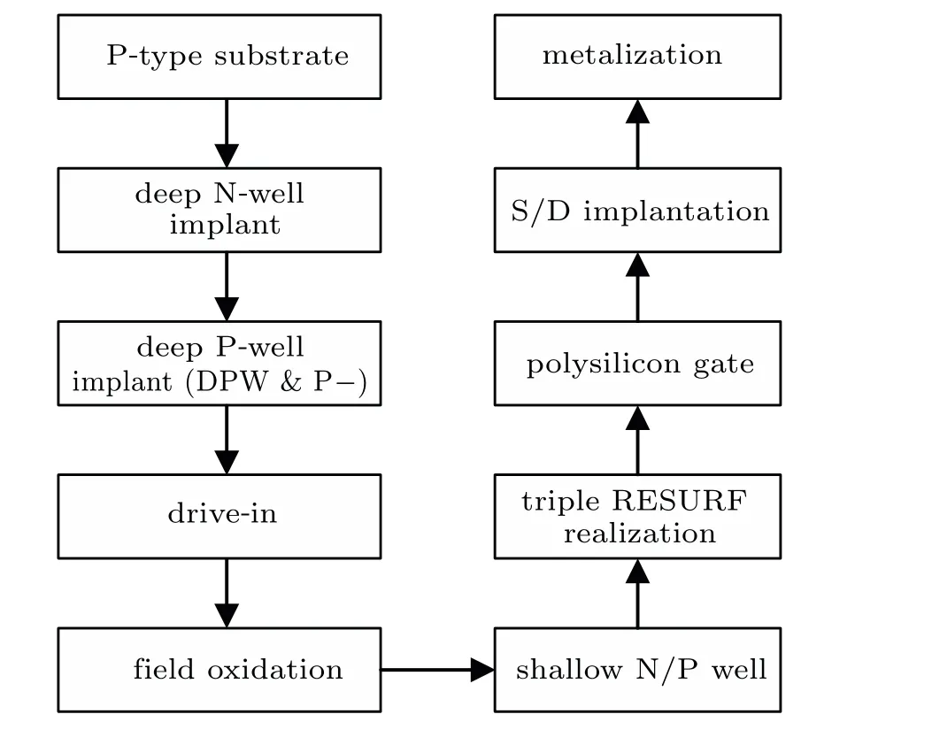
Fig.3. Process flow chart of TOTR-LDMOS.
The obtainedI–Vcurves are shown in Fig. 4. The two devices have similar leakage currents when they are in the offstate. When avalanche breakdown occurs in the reversed PN junction, the current increases rapidly, and the corresponding voltage is theBV. Comparing with the traditional LDMOS,theBVof TOTR-LDMOS increases from 755 V to 817 V,resulting mainly from the transfer of the breakdown point.
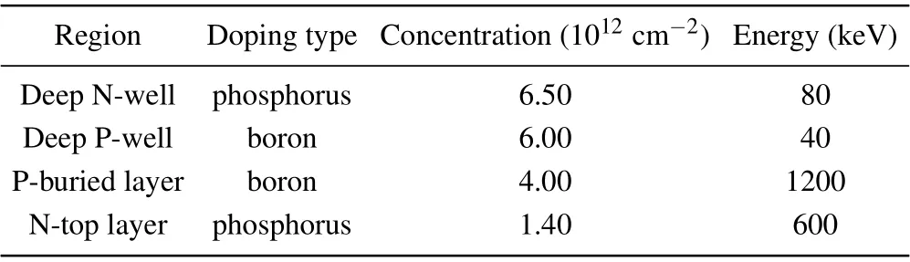
Table 1. Parameters of key layers in BCD process.
Three-dimensional (3D) TCAD simulations are conducted by Sentaurus to explore the internal physical mechanisms of the devices.Both the traditional LDMOS and TOTRLDMOS have active and terminal regions with the same sizes,consistent with their actual layouts. By applying a DC voltage to the drain, the electrostatic potential distributions before breakdown are obtained as shown in Fig. 5. The solid lines represent the equipotential lines. The denser equipotential lines correspond to the stronger electric field, where the breakdown occurs more easily.
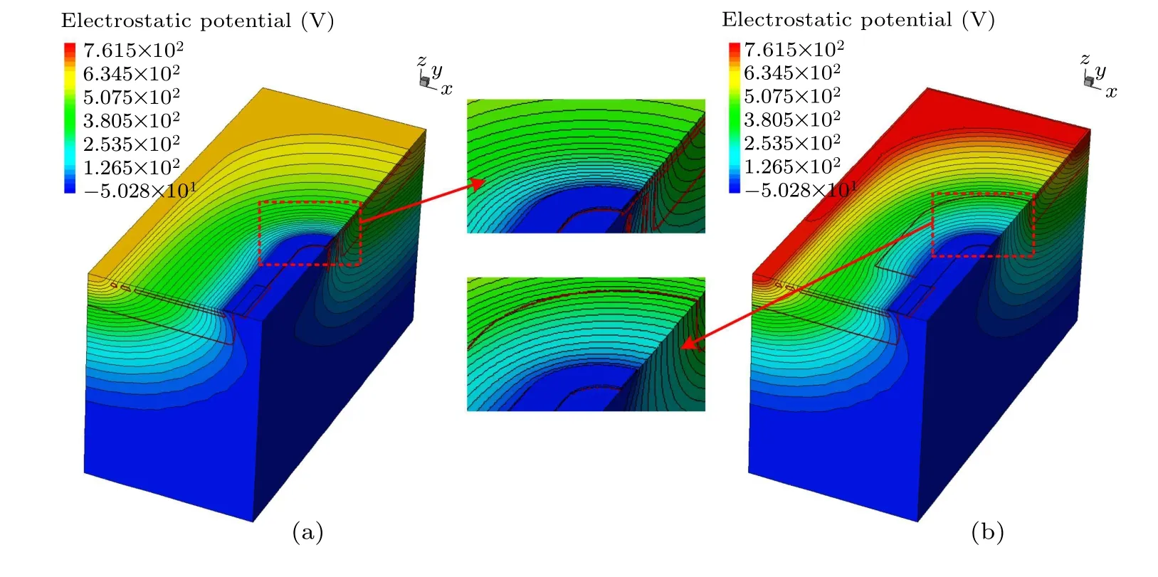
Fig.5. Simulated 3D electrostatic potential distribution in(a)traditional LDMOS and(b)TOTR-LDMOS.

Fig.4. The I–V characteristic of traditional LDMOS and TOTR-LDMOS.
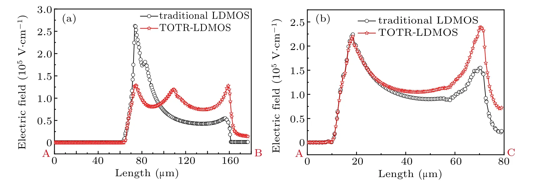
Fig.6. Surface electric field variation along(a)AB line and(b)AC line in traditional LDMOS and TOTR LDMOS.
As can be clearly seen from Fig.5(a),the terminal region in the traditional LDMOS has a denser potential distribution in the red rectangle, suggesting that the breakdown will occur first in this area under the reverse DC voltage. Compared with the traditional LDMOS,the TOTR-LDMOS possesses a very uniform distribution of electrostatic potential close to the source in terminal region,which is also sparser than that in the active region,suggesting that the breakdown will occur first in the active region. Therefore, the TOTR-LDMOS will exhibit a higherBV.
Figure 6 shows the critical breakdown electric field distribution of the traditional LDMOS and the TOTR-LDMOS along the AB line (terminal region) and AC line (active region),respectively(marked in Fig.1),which are obtained from 3D simulations. Obviously, the traditional LDMOS has an high electric field of 2.5×10⁵V/cm at a length of 75 μm in the terminal region around the source, which is much higher than that in the active region, suggesting that the traditional LDMOS breakdowns first in the terminal region. As a result,the withstanding voltage of active region in the traditional LDMOS cannot be displayed. As far as the optimized device is concerned, the position of peak electric field shifts from the terminal region to the active region,indicating that the TOTRLDMOS breakdowns first in the active region. Therefore,the TOTR-LDMOS possesses a higherBVthan the traditional LDMOS.
In order to evaluate the comprehensive performance of the TOTR-LDMOS,the following theoretical relationship between theBVandRon,spof the triple RESURF LDMOS is considered:[10]

The curve shown in Fig. 7 illustrates theBV–Ron,sprelation in a voltage range from 500 V to 900 V according to Eq. (1). The performance of proposed TOTR-LDMOS and some typical optimized LDMOS[11–14]are shown in Fig.7 and summarized in Table 2. Obviously,the difference between the TOTR-LDMOS and theoretical limit is the largest,indicating that the TOTR-LDMOS possesses the best performance in the five optimized devices.
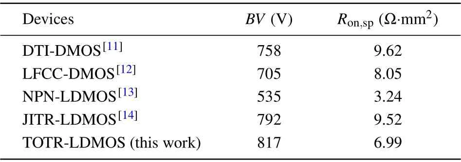
Table 2. Comparison of performance between TOTR LDMOS and other reported HV LDMOS.
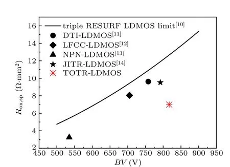
Fig.7. Comparison of BV–Ron,sp performance among five high voltage LDMOS devices.
3.2. ESD robustness
In order to verify the current discharge capacity of the TOTR-LDMOS under an ESD pulse,the TLP tests are carried out. The pulse with a rise time of 10 ns and a pulse width of 100 ns is applied to the drain of the device with the gate and source grounded. The results are shown in Fig. 8. When the leakage current increases suddenly by more than three orders of magnitude, the corresponding current is defined as theIt2,which usually reflects the ESD robustness. Comparing with the traditional LDMOS, theIt2of TOTR-LDMOS increases from 0.263 A to 0.652 A.Such a large increase by about 147%is mainly caused by the weakened current skin effect.
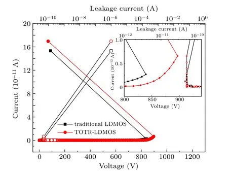
Fig.8. TLP I–V curve of traditional LDMOS and TOTR-LDMOS.
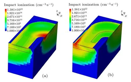
Fig. 9. Simulated impact ionization rate in (a) traditional LDMOS and (b)TOTR-LDMOS.
To confirm the weakened current skin effect, the simulated impact ionization rate distributions of both devices before thermal breakdown are shown in Fig. 9. Obviously, the traditional LDMOS collects a large amount of impact ionization in the terminal region, caused by the current skin effect,aggravating the lattice vibration,and thus resulting in the further increase of temperature. As a result, the thermal breakdown is easy to occur in the terminal region, leading to the failure of devices and circuits. Compared with the traditional LDMOS, the TOTR-LDMOS has much impact ionization in the active region instead of in the terminal region. Due to the increasedBVof terminal region, the breakdown of reversed PN junction in the active region occurs first and the device begins to discharge, thereby producing the current through the active region. The current skin effect in the terminal region is thus greatly weakened, contributing to a higherIt2for the TOTR-LDMOS.
4. Conclusions
A terminal optimized LDMOS is proposed by introducing a P-region between the deep N-well and deep P-well and fabricated in a 0.25-μm BCD process. The physical mechanism of optimization is analyzed based on testing results and 3D simulations. Compared with the traditional LDMOS, the TOTR-LDMOS has a large depletion around the optimized region, leading to a higherBVwithout significant change ofRon,sp. Meanwhile, the current skin effect in the terminal region of TOTR-LDMOS is weakened,contributing to a higher ESD robustness. As a result,The TOTR-LDMOS with a highBVof 817 V,a lowRon,spof 6.99 ?·mm2and anIt2of 0.652 A can be a promising competitor in power devices.

- Chinese Physics B的其它文章
- Coarse-grained simulations on interactions between spectrins and phase-separated lipid bilayers?
- Constraints on the kinetic energy of type-Ic supernova explosion from young PSR J1906+0746 in a double neutron star candidate?
- Computational model investigating the effect of magnetic field on neural–astrocyte microcircuit?
- Gas sensor using gold doped copper oxide nanostructured thin films as modified cladding fiber
- Exact explicit solitary wave and periodic wave solutions and their dynamical behaviors for the Schamel–Korteweg–de Vries equation?
- Suppression of ferroresonance using passive memristor emulator