
Controllable Formation of PbI2 and PbI2(DMSO)Nano Domains in Perovskite Films through Precursor Solvent Engineering
2022-03-31 12:25:16WusongZhaLianpingZhangLongWenJiachenKangQunLuoQinChenShangfengYangChangQiMa
物理化學(xué)學(xué)報(bào) 2022年3期
Wusong Zha, Lianping Zhang, Long Wen, Jiachen Kang, Qun Luo,4,*, Qin Chen,Shangfeng Yang, Chang-Qi Ma,4,*
1 Nano Science and Technology Institute, University of Science and Technology of China, Suzhou 215123, Jiangsu Province, China.
2 Printable Electronics Research Center, Suzhou Institute of Nano-Tech and Nano-Bionics, Chinese Academy of Sciences,Suzhou 215123, Jiangsu Province, China.
3 Institute of Nanophotonic, Jinan University, Guangzhou 511443, China.
4 Suzhou Institute of Nano-Tech and Nano-Bionics Nanchang, Chinese Academy of Sciences, Nanchang 330200, China.
5 Department of Materials Science and Engineering, Synergetic Innovation Center of Quantum Information & Quantum Physics,University of Science and Technology of China, Hefei 230026, China.
Abstract:Perovskite solar cells (PSCs)attract much attention for their high efficiency and low processing cost. Power conversion efficiencies (PCEs)higher than 25% have been reported in literature, demonstrating the excellent application prospect of PSCs. In general, the crystallinity and the film composition of perovskite thin films are significant factors in determining device performance. Much effort has been made to control the growth process of perovskite films through the use of additives, passivation layers, special atmosphere treatments, precursor regulation etc. Among these methods, precursor solvent engineering is a simple and direct way to control the perovskite quality, but the controllability of components through solvent engineering is still difficult and has not yet been reported. Herein, we report the controlled formation of PbI2 and PbI2 with dimethyl sulfoxide (DMSO)nano domains through precursor solvent engineering. In particular, tuning the solvent content of the dimethyl sulfoxide: 1,4-butyrolactone:N,N-dimethylformamide (DMSO : GBL : DMF)in the perovskite precursor solution, controlled the content of PbI2 and PbI2(DMSO)domains. Due to the lower boiling point and weaker coordination of DMF relative to DMSO, part of methylammonium iodide (MAI)would escape from the wet films during the evaporation process. Therefore, the PbI2(DMSO)can’t completely convert to perovskite crystals and is retained in the final films as residual PbI2(DMSO)domains. Both UV-vis absorption spectrum and XRD spectrum confirmed the existence of PbI2 and PbI2(DMSO)domains. Importantly, the content of PbI2(DMSO)was controllable by simply changing the relative proportion of DMF. With an increase in the DMF content, the residual PbI2(DMSO)domains gradually increase. In addition, the influence of PbI2 and PbI2(DMSO)domains on the device performance was systematically investigated. The formation of PbI2(DMSO)domains caused a decrease in external quantum efficiency (EQE)of the device over 300-425 nm, and consequently decreased the device performance.That was because the PbI2(DMSO)domain has strong absorption over 300-425 nm. Therefore, the PbI2(DMSO)domains would absorb the photons over 300-425 nm prior to the perovskite, however the photons absorbed by the PbI2(DMSO)domains are not converted into the photocurrent. Thus, the perovskite solar cell containing PbI2(DMSO)showed an EQE loss over 300-425 nm in the EQE spectra. This work provides a simple method to control the components, especially the content of the PbI2(DMSO)domains, in perovskite films through regulating the precursor solvent. Additionally, this work revealed a PbI2(DMSO)domain related EQE loss phenomenon, highlighting the importance of controlling this component.
Key Words:Perovskite solar cell;PbI2;PbI2(DMSO);Perovskite precursor;External quantum efficiency
1 Introduction
Perovskite solar cells (PSCs)attract much attentions for their outstanding advantages, including strong light absorption, long carrier diffusion length, tunable band structure and easy solution-based processes,etc1-4. The power conversion efficiency (PCE)of PSCs has rapidly increased from the initial 3.8% to over 25%5-8. Especially, the report of over 20% efficiency for large-area (> 1 cm2)devices9-11demonstrates the excellent application prospect in the future.
Crystalline property of the perovskite film is critical for achieving high performance perovskite solar cells12-15.Therefore, many efforts have been made in controlling the crystal growth during the formation of perovskite films though using additives16,17, surface modification18,19, component ion tuning20, as well as processing temperature optimization and so on21-24. PbI2domain is an important ingredient of perovskite, and it can passivate the boundary defects in the perovskite film25,26.Several works have been focused on the influence of PbI2domain on the device performance. Aydinet al.27demonstrated that PbI2could be easily formed in the grain boundary of perovskite crystal, which could passivate the defects of perovskite film. Zhouet al.28also revealed the passivation effect of PbI2and realized the high open circuit voltage (Voc)solar cells with 1.15 V. Youet al.29revealed the existence of moderate residual PbI2can deliver stable and high efficiency of solar cells without hysteresis. In these works, the formation of PbI2domains was almost achieved through increasing PbI2content in the precursor solution. In addition, the previous reports only revealed the effect of PbI2domains on open circuit voltage (Voc).However, the formation of perovskite crystals films is a complex reaction between PbI2and MAI from liquid phase to solid phase.Besides the original stoichiometric ratio of PbI2and MAI in the precursor, the solvent works a lot during such conversion process. However, the crystalline control through solvent regulation is rare reported.
In this work, we adopted a solvent engineering strategy to regulate the component of perovskite films by tuning the solvent ratio of DMSO:GBL:DMF in the perovskite precursor solution.The formation of PbI2and PbI2(DMSO)domains within the perovskite films was successfully controlled, and the EQE loss for the device related to PbI2and PbI2(DMSO)domains was demonstrated.
2 Experiment sections
Poly(3,4-ethylenedioxythiophene):poly(styrene sulfonate)(PEDOT:PSS Clevios PVP AI 4083)was purchased from Heraeus Precious Metals GmbH & Co. KG. MAI (99.85%), PbI2(99.95%), PbCl2(99.95%)were purchased from Xi’an Polymer Light Technology Corp. [6,6]-phenyl-C61-butyric acid methyl ester (PC61BM)was purchased from Solenne B.V.
The perovskite solar cells were fabricated according to the following procedure. Patterned indium-tin oxide (ITO)substrates were subsequently sonically cleaned in detergent aqueous solution, deionized water, acetone, and isopropanol, and finally treated in a ultraviolet ozone (UVO)for 30 min.PEDOT:PSS aqueous solution filtered through a 0.45 mm filter was spin-coated on the ITO electrode (3500 r·min-1, 60 s), and then baked at 140 °C in air for 10 min. After that the ITO/PEDOT:PSS substrates were then transferred to a nitrogenfilled glove-box for the deposition of perovskite layer.
Methylammonium iodide (MAI, 206.7 mg), lead iodide (PbI2,613.1 mg)and lead chloride (PbCl2, 38.9 mg)were stirred in 1 mL of mixture solvent at 60 °C for 3 h, and the mixture solvent is made up of dimethyl sulfoxide (DMSO, HPLC, Aladdin), 1,4-butyrolactone (GBL,HPLC,Aladdin) andN,N-dimethylformamide (DMF, HPLC, Aladdin)with a ratio of 0.3 :(0.7 -x):x, volume fraction,x= 0, 0.05, 0.1, 0.15, 0.2, 0.25.Inside the glovebox, the resulting solution was spin coated by a consecutive two step spin-coating process at 1000 r·min-1for 10 s, and 4000 r·min-1for 20 s. During the spin-coating step at 28 s after the beginning of the spin coating, anhydrous toluene (450 mL)was quickly dropped onto the center of the films. The substrate was annealed on a hotplate at 100 °C for 10 min to form a CH3NH3PbClxI3-xfilm. The PC61BM layer was spin coated on the perovskite layer at 1800 r·min-1for 60 s from the PC61BM solution (25 mg·mL-1in CB). Finally, 100 nm Al electrode was evaporated deposited at vacuum degree of 4 × 10⁻⁴Pa.
Layer thickness of the perovskite films were measured by an Alpha Step profilometer (Veeo, Dektak 150); The XRD spectra of the perovskite films were obtained by a Bruker D8 Advance X-ray diffractometer with CuKαradiation (λ= 0.15418 nm). The UV-Vis absorption spectra were recorded with a Lambda 750 UV-Vis NIR Spectro-photometer (PerkinElmer). The current density-voltage (J-V)curves were measured using a Keithley 2400 under simulated AM 1.5G sun light illumination (100 mW·cm-2).
External quantum efficiencies (EQE)were measured under simulated one sun operation conditions using a bias light of 532 nm from a solid-state laser (Changchun New Industries, MGLIII-532). Light from a 150 W tungsten halogen lamp (Osram 64642)was used as probe light and modulated with a mechanical chopper before passing the monochromator (Zolix, Omni-l300)to select the wavelength. The response was recorded as the voltage by anI-Vconverter (QE-IV Convertor, Suzhou D&R Instruments), using a lock-in amplifier (Stanford Research Systems SR 830). A calibrated Si cell was used as reference. The test device was kept behind a quartz window in a nitrogen filled container.
3 Results and discussion
As shown in Fig. 1a, the perovskite solar cell with structure of ITO/PEDOT:PSS/Perovskite/PC61BM/Al was fabricated as research model. PEDOT:PSS was coated on ITO layer, and perovskite, PC61BM, Al layers were deposited layer by layer.Ternary mixed solvent of DMSO:GBL:DMF was used to dissolve perovskite precursor and control the component of perovskite films. By regulating the volume ratio of DMF from 0% to 25%, a series of perovskite solar cells (PSCs)have been fabricated. Fig. 1b,c show theJ-Vcurves and EQE spectra of the perovskite solar cells, and the statistical photovoltaic performance data are listed in Table 1. As seen here, with the increase of content DMF from 0% to 25%, the open circuit voltage (VOC)showed slight change (around 1.00 V, Table 1). In case of short circuit current density (JSC)of the devices, we also found slight change. In detail,JSCincreased from 18.83 mA·cm-2(0% DMF)to 19.51 mA·cm-2(10% DMF), and then fall to 19.29 mA·cm-2(25% DMF). The fill factor (FF)changed a little as the content of DMF was within 20%. As a result, with the increase of DMF content from 0% to 25%, the power conversion efficiency (PCE)of devices first rose from 13.31% (0% DMF)to 14.05% (10% DMF), and then decreased to 12.41% (25% DMF), with a saturation at 10% DMF. This result indicated similar device performance could be obtained through regulating the content of DMF in the precursor solution as long as the content of DMF was controlled within a certain range.
Table 1 Device performance of the perovskite solar cells.
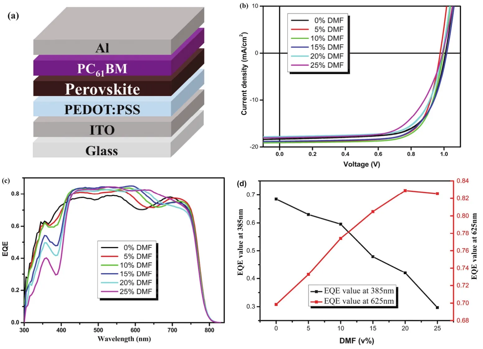
Fig. 1 (a)The device structure, (b)J-V curves, (c)EQE spectra of the perovskite solar cells, and (d)Evolution of EQE value at 385 and 625 nm.
However, the EQE spectra (Fig. 1c)shows interesting variation for these devices. As showed in this figure, a regular decrease of EQE from 300 to 450 nm was observed. In contrast,from 550 to 750 nm, EQE values increased gradually with the increase of DMF content. Meanwhile, a gradual red shift in the response edge around 700 nm was observed as well. Because of the different change tendency of these device in short wavelength and long wavelength regions, the dependence of EQE value on the content of DMF was drew in Fig. 1d.
As illustrated above, the regulation of DMF content in the precursor solution would cause the decrease of EQE value in 300-450 nm, while increase the EQE value in long wavelength region. In order to reveal the reason of DMF content dependent-JSCchange, we firstly measured the layer thickness of the perovskite films and investigated the impact of thicknesses on the performance. As the result showing in Table 1, with the increase of DMF content, the layer thickness of the perovskite film increased gradually from 290 to 367 nm. Knowing DMF has lower boiling point (152.8 °C)than DMSO (189 °C)and GBL (204°C)24,30, the fast evaporation of DMF would lead to the fast formation of perovskite layer, which was ascribed to the main reason for the increase of layer thickness. A thicker perovskite layer could enhance absorption31,32and improve the EQE value33,34. To better understand such relationship between the thickness of perovskite layer and EQE results, the simulation of EQE was showed in Fig. 2. Optical simulation showed that,with the increase of DMF content from 0% to 25%, a red shift of EQE curve over 550-750 nm was detected for the cells.Meanwhile, the EQE intensity from 600 to 800 nm increased for the thicker perovskite film. This result was corresponded with the experiment result. However, in range of 350 to 425 nm, all of the devices had the same EQE value in simulation result.Based on the optical simulation result we know the EQE regular decrease over 350-425 nm is not due to the optical effect caused by layer thickness.
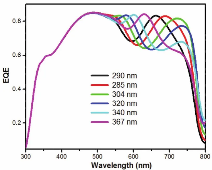
Fig. 2 Simulation EQE spectra of PSCs with different thickness perovskite thin films.
Further, we measured the XRD patterns of the perovskite films with different DMF contents. As showed in Fig. 3a, all the films display diffraction peaks at 14.08°, 28.41°, 31.85°,corresponding to (110), (220), (310)planes of the CH3NH3PbI3-xClxcrystals35,36, indicating the formation of orthorhombic crystal structure of the perovskite films37. In addition, we found the halfwidth of diffraction peak of the 15% DMF films were slight narrower than that of the film w/o DMF,suggesting increased crystal size. Similar results were observed in the SEM images (Fig. S1, Supporting Information)of these films. This result is reasonable because the weaker coordination of DMF with PbI2would lead to faster growth rate of perovskite crystals. In addition, a diffraction peak at 12.65° that can be assigned to the crystal of PbI2was detected in these films,indicating the formation of PbI2crystals in perovskite films38,39.In addition, with increase of DMF content, a diffraction peak at 9.20° was observed, which could be ascribed to PbI2(DMSO)39,40.Fig. 3b shows the diffraction peak changing tendency of PbI2(DMSO)(9.20°)and PbI2(12.65°). With DMF content increasing, the PbI2(DMSO)diffraction peak at 9.20° increased gradually, while the PbI2diffraction peak changed less. Since the change tendency of the PbI2(DMSO)diffraction peaks intensity exhibited the same variation of EQE decrease in 300-450 nm,the formation of PbI2(DMSO)might be the reason of EQE loss.
Fig. 3 (a)XRD patterns of the perovskite films and (b)PbI2/PbI2(DMSO)diffraction peak changing tendency with different DMF contents.
In order to confirm the relation of PbI2(DMSO)domain and EQE decrease, we carefully analyzed the EQE spectra. The EQE difference spectrum between the control sample and the DMF-based sample was obtained through reducing EQE value by that of the reference sample (0% DMF). The results are showed in Fig. 4a. With the increase of the DMF content from 5% to 25% DMF, the difference intensity enhanced gradually. It indicated the EQE loss over 350-450 nm increased gradually with the increasing of DMF solvent. Knowing the perovskite solar cells have strong light harvest and conversion ability, the EQE loss in the wavelength of 300-450 nm might be ascribed to the formation of other materials which has low photoelectric response in 350-450 nm33,41,42. Fig. 4b shows the absorption spectra of the PbI2(DMSO). In this figure, one can find PbI2(DMSO)has strong absorbance over 400-500 nm.Especially, an absorption cut-off edge at 425 nm was observed.This absorption band of PbI2(DMSO)was in good agreement with the EQE loss in 300-450 nm, so the existence of PbI2(DMSO)maybe the reason of EQE loss43. In other words,with the DMF content increasing from 0% to 25%, the residual PbI2(DMSO)leads to the EQE loss over 350-450 nm.
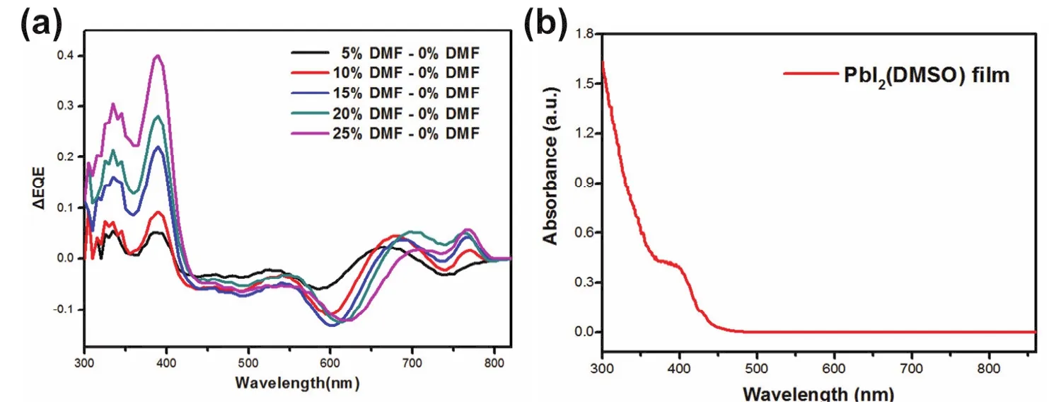
Fig. 4 (a)EQE difference spectrum and (b)absorbance of PbI2(DMSO).
It can be seen from the above conclusion that the residual PbI2(DMSO)can lead to the EQE loss over 350-450 nm. The possible mechanism was given in Fig. 5. The formation process of perovskite films from precursors could be described as follow:the dissolved PbI2would mainly form PbI2(DMSO)colloidal in the solution due to strong coordination ability of DMSO. After spin-coating, PbI2(DMSO), PbI2and MAI co-existed in the wet film. Chemical reaction between PbI2(DMSO)/PbI2and MAI occurred during the thermal annealing process and converted to perovskite crystals. With the addition of DMF in the precursor solution, more MAI would escape from the wet films during the evaporation process of DMF relative to the case of without DMF,since DMF had lower boiling point (152.8 °C)than DMSO (189°C)and GBL (204 °C). The loss of MAI in the wet films then caused un-complete conversion from PbI2(DMSO)/PbI2to perovskite. Consequently, the Pb2(DMSO)domain remained in the perovskite films. With increase of DMF content, more MAI was lost, leading to more residual Pb2(DMSO)domain. The DMF content-dependent XRD and device performance results were highly related to the Pb2(DMSO)domain.
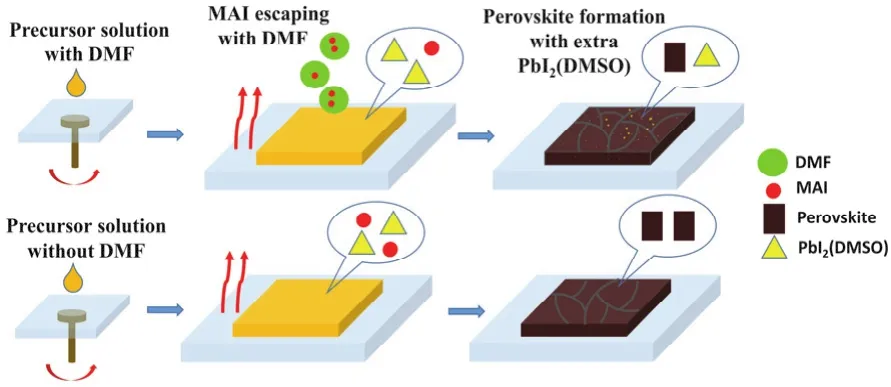
Fig. 5 Schematic diagram of DMF leading the formation of PbI2(DMSO)domains.
Since PbI2(DMSO)is an intermediate phase formed during the crystallization of perovskite phase, we tried to remove this phase through thermal annealing. For case of 20% DMF precursor, a series of perovskite films annealed for different time were fabricated, and Fig. S2 showed the EQE spectra of these cells. The results showed an increasing tendency of EQE spectra over 350-450 nm, which indicated that the PbI2(DMSO)intermediate phase can be controlled by thermal annealing.However, when the annealing time increases from 6 to 10 min,the EQE spectra showed negligible change over 350-450 nm,demonstrating the PbI2(DMSO)domains couldn’t be completely removed trough prolonging annealing time for this sample. In addition, the formation of perovskite is depended on the reaction between MAI and PbI2, so increasing the MAI ratio in the perovskite precursor solution can also reduce the extra PbI2(DMSO)44,45. Herein, we used the ternary mixture solvent(DMSO:GBL:DMF)of 3 : 5 : 2 (volume ratio)to dissolve different ratios of MAI and PbI2to prepare the precursors.Specifically, the ratio of MAI and PbI2is from 1.2 mol·L-1: 1.4 mol·L-1(1.2M : 1.4M)to 1.45M : 1.4M. XRD patterns of the perovskite films are shown in Fig. 6. As seen here, all the films have diffraction peaks at 14.08°, 28.41°, 31.85°, corresponding to (110), (220), (310)planes of the CH3NH3PbI3-xClxcrystals,indicating the formation of orthorhombic crystal structure of the perovskite films. This result confirmed that the addition of MAI could not change the perovskite structure, which was in keeping with the result of changing DMF content. However, the diffraction peak of 9.20° decreased gradually with the increasing of MAI ratio. When the concentration of MAI comes to 1.45M,MAI : Pb = 1.45M : 1.4M, the diffraction peaks of 9.20° and 12.65° were not observed, which demonstrated the extra PbI2(DMSO)and PbI2have been converted into perovskite totally.
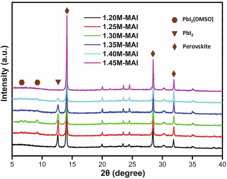
Fig. 6 XRD patterns of the perovskite films prepared from the precursor solution with different ratio of MAI to PbI2.
The XRD result proved that increasing MAI ratio in perovskite precursor could reduce the extra PbI2(DMSO).Correspondingly, we fabricated the perovskite solar cells with these films. Fig. 7 shows theJ-Vcurves and EQE spectra, and the statistical photovoltaic performance data are listed in Table 2. Herein, the thickness of perovskite layers was similar. With the increase of MAI content, the EQE spectra over 350-450 nm increased gradually, demonstrating that the MAI can reduce the extra PbI2(DMSO), which is correspond to the XRD results.Meanwhile, theVOCof the devices decreased from 1.05 V (MAI: PbI2= 1.2M : 1.4M)to 0.72 V (MAI : PbI2= 1.4M : 1.4M), and then came to 1.00 V with the ratio of MAI to PbI2was 1.45M :1.4M. We know nonradiative recombination due to various films defect is a main origin ofVOCloss. So, improving the films quality and passivating the films defects are two strategies to achieve highVOC. PbI2can effectively passivate the films defects, and thus improve the deviceVOC28. In these cases of MAI : PbI2= 1.2M : 1.4M, 1.25M : 1.4M, 1.30M : 1.4M, 1.35M :1.4M, and 1.40M : 1.4, the XRD patterns of these films all showed the existence of excess PbI2. Therefore, the defect passivation effect by PbI2would be expected in these films. With the increase of MAI content, the content of PbI2decrease gradually, thereby insufficient defect passivation by less PbI2lead to lowerVOC. As the ratio of MAI to PbI2increased to 1.45M: 1.4M, pure perovskite phase was observed in the XRD patterns.The sharp increase ofVOCmight imply the improved crystal quality and less films defects of the perovskite films as compared to other films.
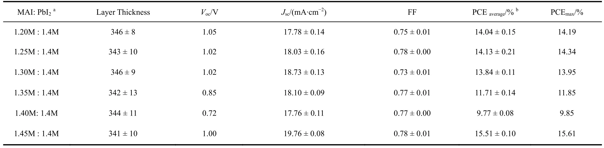
Table 2 Device performance of the perovskite solar cells.
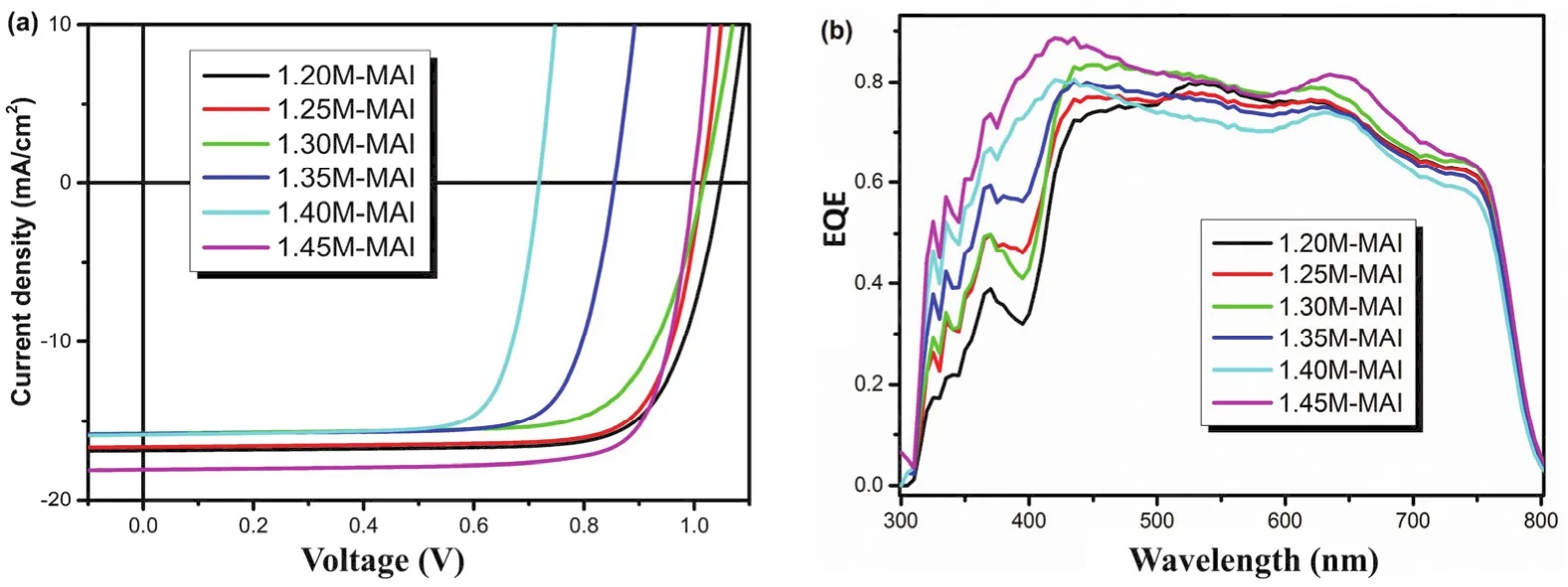
Fig. 7 J-V curves (a)and EQE spectra (b)of perovskite solar cells with different MAI concentrations.
4 Conclusions
In this work, we adopted a solvent engineering strategy to regulate the component and thickness of perovskite films. By varying the DMF concentration of the perovskite precursor solutions in the mixed solvents of DMSO:GBL:DMF, the content of PbI2(DMSO)domains and the films thickness were systematically regulated. Both UV-vis absorption spectrum and XRD spectrum proved the existence of PbI2(DMSO)domains,which decreased the devices EQE over 300-450 nm. Finally, by increasing the ratio of MAI in perovskite precursor solution, the residual PbI2(DMSO)would transform to perovskite completely and the power conversion obtained a higher enhancement to 15.61%. This work provided a new solvent engineering strategy to in-situ tune the formation of PbI2and PbI2(DMSO)domains in perovskite films.
Supporting Information:available free of chargeviathe internet at http://www.whxb.pku.edu.cn.

- 物理化學(xué)學(xué)報(bào)的其它文章
- Seeding and Cross-Seeding Aggregations of Aβ40 and hIAPP in Solution and on Surface
- High-Performance Palladium-Based Catalyst Boosted by Thin-layered Carbon Nitride for Hydrogen Generation from Formic Acid
- Eu(III)在蒙脫石上的吸附及碳酸根和磷酸根對(duì)其吸附的影響
- 鋯合金初始氧化行為的原位近常壓XPS研究
- Methanol Synthesis by COx Hydrogenation over Cu/ZnO/Al2O3 Catalyst via Hydrotalcite-Like Precursors: the Role of CO in the Reactant Mixture
- 自交聯(lián)共軛亞油酸囊泡基熒光納米點(diǎn)的構(gòu)筑及其熒光特性