
Improving the performance of a GaAs nanowire photodetector using surface plasmon polaritons
2022-04-12 03:45:02XiaotianZhu朱笑天BinghengMeng孟兵恒DengkuiWang王登魁XueChen陳雪LeiLiao廖蕾MingmingJiang姜明明andZhipengWei魏志鵬
Chinese Physics B 2022年4期
Xiaotian Zhu(朱笑天) Bingheng Meng(孟兵恒) Dengkui Wang(王登魁) Xue Chen(陳雪)Lei Liao(廖蕾) Mingming Jiang(姜明明) and Zhipeng Wei(魏志鵬)
1State Key Laboratory of High Power Semiconductor Lasers,Changchun University of Science and Technology,Changchun 130022,China
2State Key Laboratory for Chemo/Biosensing and Chemometrics,School of Physics and Electronics,Hunan University,Changsha 410082,China
3College of Science,Nanjing University of Aeronautics and Astronautics,Jiangsu 210016,China
Keywords: GaAs nanowire(NW),capsule-like Au nanoparticles,photodetector,surface plasmon polariton
1. Introduction
Quasi-one-dimensional GaAs nanowires (NWs) are desirable in high-performance photodetectors owing to their superior properties, such as a direct band gap as high as 1.42 eV, fast carrier mobility and high compatibility with Si technology.[1-3]Research on GaAs NW photodetectors has made rapid progress in the past decade.[4-6]At present, the dark current of such devices has been reduced by surface passivation,[7]However, there is a significant gap in research on how to effectively improve the photocurrent of these devices.
Surface plasmon polaritons (SPPs) represent a phenomenon in which free electrons at the interface between metal materials and air are excited by light to produce collective oscillations.[8-12]The SPP mode can confine the incident light to the surface of metal material and make it propagate along the metal surface. This limiting effect significantly increases the intensity of the electromagnetic field at the interface.[13-19]Au nanoparticles have been used in the visible band.[20-22]However,the enhancement effect of SPPs realized by Au nanoparticles on the photoresponse in the infrared band is not clear.[23,24]A comparison of the performance of photodetectors based on GaAs before and after SPP treatment is also lacking.
In this study, we placed capsule-like Au nanoparticles with absorption edges of approximately 800 nm on the surface of p-type GaAs NWs. The performance of the device was thus significantly improved under an 808 nm excitation light source: the responsivity and detectivity increased by a factor of 3.2 to 6.56 A·W-1and 2.53 to 5.6×10¹⁰Jones, respectively. This improvement in the device performance was due to the specific wavelength selectivity. From the perspective of compatibility between plasma and dielectric materials,this study improves the photoresponse performance of GaAs NW photodetectors and expands the application prospects of SPPs.
2. Experiment
2.1. NW growth
Using a DCA P600 molecular beam epitaxy(MBE)system, GaAs NW arrays were synthesized on an undoped Si(111)substrate by a Ga-assisted autocatalytic growth mode at 600°C and a V/III beam ratio of 25(Ga beam equivalent pressure (BEP) of 6.4× 10⁻⁸Torr, As BEP of 1.6×10⁻⁶Torr,1 Torr=133.322 Pa). The GaAs NW used was approximately 200 nm in diameter and 7μm long(see Fig.S1 in the supplementary information).
2.2. Preparation and testing of the NW photodetector
A 1 cm×1 cm substrate of p+ Si/SiO2(100 nm thick)was first prepared. After ultrasonic treatment with alcohol,acetone and deionized water for 15 min, the substrate surface was dried with nitrogen to achieve a clean and pollutionfree surface. Then, another substrate with a GaAs NW array was buckled onto the prepared substrate; tweezers were used to gently slide the upper substrate allowing the GaAs NWs to slide off to the lower substrate.[25]Au nanoparticles were attached to the surface using a droplet method. Then,polymethyl methacrylate and methyl methacrylate were spin coated on the surface, followed by electron beam etching(EBL; JEOL 6510 with a nanometer pattern generation system).Finally,a Cr/Au(15 nm/100 nm)electrode was prepared by thermal evaporation, and a Schottky-Ohmic contact photodetector was obtained. After device fabrication, the photoelectric performance of the GaAs NW photodetector was measured using an Agilent 4155C semiconductor analyser. The morphology of the GaAs NWs was characterized by a JSM-6510 scanning electron microscope(SEM).
3. Discussion
Figure 1 depicts the fabrication process for a single GaAs NW photodetector. Figure 1(a) shows a SEM image of the GaAs NW arrays grown by MBE. It is apparent that the diameter of the GaAs NWs is approximately 200±10 nm, and that they have a hexagonal structure. Figure 1(b)shows a single GaAs NW transferred to the substrate for photolithography by mechanical stripping. Figure 1(c)shows Au nanoparticles dissolved in deionised water and then dropped on the surface of the GaAs NWs. The illustration shows the SEM image of the capsule-like Au nanoparticles. It can be clearly observed that the length to diameter ratio of the Au nanoparticles is approximately four, the length is approximately 80 nm and the width is approximately 20 nm. Finally, a single GaAs NW photodetector was fabricated by EBL, spin coating and thermal evaporation processes. Figure 1(d)shows SEM images of the device.The SEM image shows that many Au nanoparticles become attached to the surface of GaAs NWs.
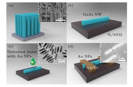
Fig.1. Schematic diagram of the preparation of a single GaAs NW photodetector. (a)A GaAs NW array;the inset is the SEM image. (b)Transfer of a single GaAs NW.(c)Au nanoparticles are attached to the surface of a GaAs NW;the inset is the SEM image of Au nanoparticles. (d)A single GaAs NW photodetector;the inset is the SEM image.
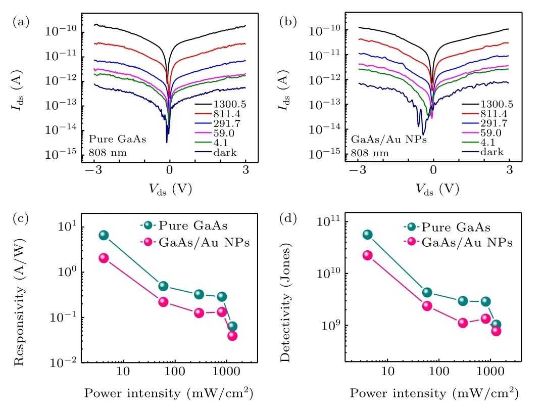
Fig. 2. (a), (b) The I-V characteristics of GaAs NW photodetectors before and after attachment of Au nanoparticles under 808 nm excitation(unit mW·cm-2). (c),(d)R and D?of the device before and after treatment.
TheI-Vcharacteristics of the GaAs NW photodetectors before and after treatment under an 808 nm excitation light source were tested, and the responsivity (R) and detectivity(D?) calculated, as shown in Fig. 2. Figures 2(a) and 2(b)show the photoresponse characteristics of the single GaAs NW photodetector with different excitation powers before and after the attachment of Au nanoparticles,respectively. It is evident that the photocurrent of the device increases with increase in the excitation power, but the increase in amplitude decreases gradually. This is because the carriers in the GaAs NWs tend to saturate gradually. The asymmetry between photocurrent and dark current curves is due to the difference in the Schottky barrier between the two electrodes. Under an excitation power of 4.1 mW·cm-2,the photocurrent of the device(Ilight)changed from 1.38×10⁻¹²A to 2.92×10⁻¹²A and the dark current(Idark)changed from 6.42×10⁻¹³A to 6.9×10⁻¹³A.The increase inIlightis due to the enhanced absorption of the excitation source by SPPs.Figure 2(c)showsRfor two groups of devices under different excitation powers.Ris the physical quantity used to describe the photoelectric conversion capability of the device.[26]With increase in the excitation power,Rof the devices gradually decreases,similar to the current change.The formula is
whereAis the photosensitive area andPis the incident light power density (mW·cm-2). TheRvalues of the two devices are 2.05 A·W-1and 6.56 A·W-1,andRis increased by a factor of 3.2. Another important performance parameter of the photodetector,D?, is shown in Fig.2(d); this is used to characterize the ability of the device to detect weak signals.[27]The formula is
whereeis the unit charge (1.6×10⁻¹⁹C). TheD?values of the two devices are 2.24×10¹⁰Jones and 5.6×10¹⁰Jones,respectively,a factor of 2.53 increase.
TheI-Vcharacteristics of the GaAs NW photodetector before and after treatment were tested under a 532 nm excitation light source, andRandD?were calculated as depicted in Fig. 3. The current of the device before and after treatment increases with increase in the excitation power,as shown in Figs. 3(a) and 3(b). Under an excitation power of 4.1 mW·cm-2,Ilightof the device changed from 1.35×10⁻¹²A to 2.2×10⁻¹²A andIdarkchanged from 6.61×10⁻¹³A to 5.4×10⁻¹³A. Compared with theI-Vcharacteristics under 808 nm excitation, the overall photocurrent of the device under 532 nm excitation is slightly smaller. This is because the excitation wavelength of 808 nm is closer to the cut-off wavelength of GaAs. Figures 3(c) and 3(d) showRandD?of the device before and after treatment.RandD?of the device increased from 1.35 A·W-1to 3.2 A·W-1and from 1.47×10¹⁰Jones to 3.06×10¹⁰Jones,respectively. Au nanoparticles with an aspect ratio of four can improve the absorption intensity at 800 nm.
We also compared the performances of various GaAsbased photodetectors reported in the literature(Table 1).Compared with other photodetectors,the capsule-like Au nanoparticles effectively enhanced the photocurrent and responsivity of GaAs NW photodetectors.
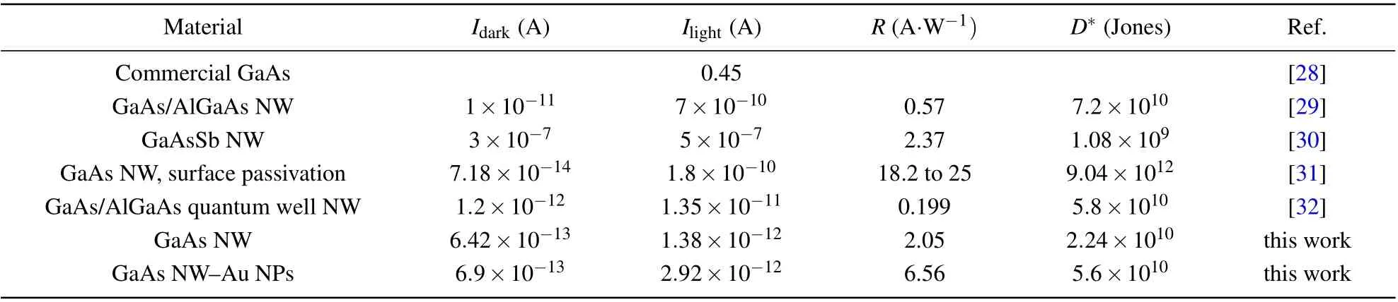
Table 1. Performance comparison of GaAs-based NW photodetectors.
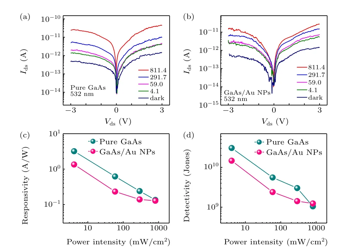
Fig. 3. (a), (b) The I-V characteristics of GaAs NW photodetectors before and after Au nanoparticle attachment under 532 nm excitation (unit mW·cm-2). (c),(d)R and D?of the device before and after treatment.
To confirm the source of the improved performance, we first simulated the absorption spectrum of a single Au nanoparticle using FDTD solutions,as shown in Fig.S2. The simulation results show that the absorption peak of Au nanoparticles is approximately 800 nm,which is consistent with our prediction. Figure 4(a)illustrates the band diagram of the GaAs NW with Au nanoparticles. When the excitation light source irradiates Au nanoparticles,the nanoparticles absorb light energy and produce hot carriers. The hot holes will transfer towards the contact p-type GaAs NWs,forming a photocurrent and enhancing the photoresponse under the applied bias.[28-30]To verify whether the capsule-like Au nanoparticles can enhance the absorption of GaAs NWs at 808 nm,we tested the absorption spectra of GaAs NWs before and after placement of the Au nanoparticles, as depicted in Fig. 4(b). The figure shows that that capsule-like Au nanoparticles have the strongest absorption intensity near 800 nm (black line), and pure GaAs NW has the strongest absorption intensity at approximately 870 nm,which corresponds to the cut-off wavelength of GaAs(red line).[31]After treatment, the overall absorption strength of the NWs was improved(cyan line). Moreover,the absorption curve after treatment minus the absorption curve before treatment (gray dashed line), and its change law, are similar to the Au nanoparticle curve. In particular,the absorption intensity near 800 nm is the highest, owing to the role of Au nanoparticles. Therefore, the capsule-like Au nanoparticles exhibit a specific absorption of 800 nm.
Finally, to evaluate the switching response (on state and off state)of the photodetector,the transient photoelectric current (TPC) of the GaAs NW photodetector before and after treatment under 808 nm excitation is tested,[37]as demonstrated in Fig. 5. The response time of the device is defined as the time for the photocurrent signal to increase from 10%to 90% (rise time) and to decrease from 90% to 10% (decay time). In this study,the rise and decay times of the pure GaAs NW photodetector at 808 nm are 19 ms and 66 ms, respectively, as shown in Fig. 5(a). After treatment, the rise and decay times are 16 ms and 103 ms, respectively, as shown in Fig. 5(b). As depicted by the TPC, the photocurrent of the device is improved by the addition of Au nanoparticles.[8,38]
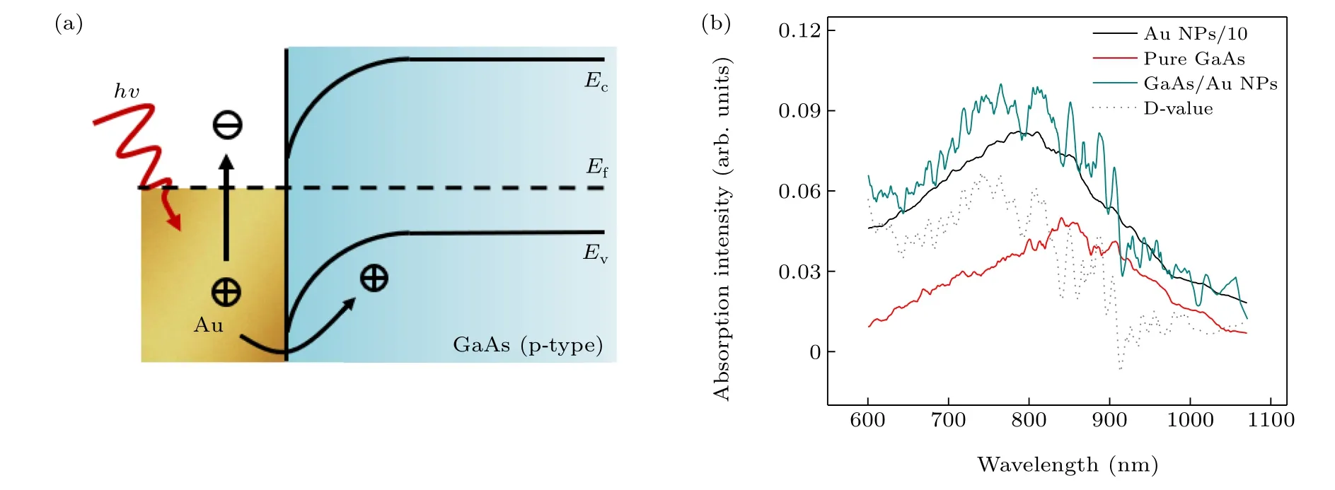
Fig.4. (a)Schematic diagram of the energy bands of GaAs NWs with Au nanoparticles. (b)Absorption spectra of GaAs NWs before and after the attachment of Au nanoparticles.
Fig. 5. (a), (b) Transient photoelectric current of a single GaAs NW photodetector before and after the attachment of Au nanoparticles under excitation at 808 nm. The illustration shows three periods.
The illustration shows the transient response of the device in three cycles, indicating that the device possesses good stability and repeatability. The response time rule under 532 nm excitation is the same,as shown in Fig.S2.
4. Conclusion
In summary,we prepared a single GaAs NW photodetector and placed capsule-like Au nanoparticles on its surface.By calculating the photoelectric characteristics and performance of the device, we confirmed that the excitation light source is close to the cut-off wavelength of the material; the device will thus generate more photogenerated carriers. Additionally,the capsule-like Au nanoparticles were selected according to the excitation band of GaAs NWs, which played the role of SPP to a great extent. Under the excitation of a 808 nm light source,Rof the treated device was increased by a factor of 3.2 to reach 6.56 A·W-1andD?was increased by a factor of 2.53 to 5.6×10¹⁰Jones. Therefore,this study expands the possible applications of SPPs.
Acknowledgments
Project supported by the National Natural Science Foundation of China(Grant Nos.62074018, 12074045, 61904017 and 11804335), the Developing Project of Science and Technology of Jilin Province,China(Grant No.20200301052RQ),and the Project of Education Department of Jilin Province,China(Grant Nos.JJKH20200763KJ and JJKH20210831KJ).
- Chinese Physics B的其它文章
- Helium bubble formation and evolution in NiMo-Y2O3 alloy under He ion irradiation
- Dynamics and intermittent stochastic stabilization of a rumor spreading model with guidance mechanism in heterogeneous network
- Spectroscopy and scattering matrices with nitrogen atom:Rydberg states and optical oscillator strengths
- Low-overhead fault-tolerant error correction scheme based on quantum stabilizer codes
- Transmembrane transport of multicomponent liposome-nanoparticles into giant vesicles
- Molecular dynamics simulations of A-DNA in bivalent metal ions salt solution