
Ultra-broadband absorber based on cascaded nanodisk arrays
2022-04-12 03:44:16QiWang王琦RuiLi李瑞XuFengGao高旭峰ShiJieZhang張世杰RuiJinHong洪瑞金BangLianXu徐邦聯andDaWeiZhang張大偉
Chinese Physics B 2022年4期
Qi Wang(王琦), Rui Li(李瑞), Xu-Feng Gao(高旭峰), Shi-Jie Zhang(張世杰),Rui-Jin Hong(洪瑞金), Bang-Lian Xu(徐邦聯), and Da-Wei Zhang(張大偉)
Engineering Research Centre of Optical Instrument and System,the Ministry of Education,Shanghai Key Laboratory of Modern Optical System,University of Shanghai for Science and Technology,Shanghai 200093,China
Keywords: ultra-broadband absorption,cascaded nanodiskarrays,polarization-independent
1. Introduction
Nanotechnology develops rapidly.[1-5]Ultra-broadband absorbers exhibit great potential applications in the optoelectronic devices,such as photodetectors,infrared cloaking,solar cells,imaging.[6,7]Generally,most perfect absorptions are designed into metal-insulator-metal (MIM) structures.[8]However, the conventional three-layer MIM absorbers contribute to narrow bandwidths due to their resonant characteristics.To extend the absorption bandwidth, several different aspects have been studied widely, such as incorporating multi-sized resonators and multi-thickness metasurfaces.[9]Furthermore,strips,[10]squares,[11]disks,[12]and crosses[13]within a unit cell have also been investigated. Nevertheless,the bandwidths of these absorbers are limited by the possible number of resonators that can be integrated into the unit cell.
Recently, the nanostructures designed by graded nonnoble metal/dielectric patterns with many stacks have been proposed to broaden the bandwidth. For example, Wanget al.[14]demonstrated an ultra-broadband,omnidirectional,and polarization-insensitive absorber based on cascaded nanorod arrays (CNAs), which achieved an average absorptivity of 98.2%with a relative absorption bandwidth(RAB)of 149.8%in a wavelength range of 0.38μm-2.65μm. Liuet al.[15]proposed an ultra-broadband perfect absorber (UBPA) by utilizing a multi-size rectangular structure,consisting of multi-layer silicon/iron(Si/Fe)units,which possesses an average absorptivity of over 96% in a range of 300 nm-3000 nm under the normal incidence. The materials are non-noble metals which reduce the cost. However, the number of layers is over 10,which brings a great challenge to the process of fabrication. In practical applications,it is desirable for an absorber to own not only an ultrabroad bandwidth,high absorption efficiency,and compact device size but also simplicity fabrication and low cost.
Here, we propose an omnidirectional absorber consisting of cascaded nanodisk arrays by placing an insulatormetal-insulator-metal(IMIM)nanodisk on an insulator-metal film stack, which can exhibit ultra-broadband, good angleinsensitive properties and polarization-independent characteristics in the near-infrared region. Additionally,simulation results indicate that an average absorption of over 91.5% can be achieved at wavelengths ranging from 600 nm to 4000 nm.With the analyses of the electric and magnetic field distributions, we first illustrate that the physical basis for the ultrabroadband absorption is contributed to from the localized surface plasmons (LSPs), propagating surface plasmons (PSPs),and plasmonic resonant cavity(PRC)modes. Then,we calculate the impedance of the designed structure, compare it with that of the corresponding six-layer metal-insulator film stack,which is analyzed for understanding the absorption physical mechanism. To further investigate its absorption performance,the influences of different disk radii and metal materials on the absorption characteristics are also investigated for comparison. Moreover,the polarization-independent characteristic is manifested due to its symmetry structure. Finally, the broadband absorption features can be well maintained at the incident angle of up to 40°for both transverse magnetic(TM)polarization and transverse electric (TE) polarization. All these impressive absorption properties make our proposed structure suitable for wide applications such as in photovoltaic devices,remote sensing,and photodetectors.
2. Structure and method
The side view of the broadband absorber is displayed in Fig. 1(a). The absorber consists of an Al2O3-Ti-Al2O3nanodisk array(h1=120 nm,h2=30 nm,R2=100 nm)on the top,a bottom Ti nanodisk array(h2=30 nm,R1=100 nm),a thin Al2O3dielectric layer(h1=120 nm)in the middle,and an opaque Ti substrate(h3=220 nm)at the bottom. Figure 1(b)is the schematic diagram of the broadband absorber. The nanodisk array is symmetrical along thexandydirections. Therefore,Λ=210 nm is the period in thexandydirections. The bottom Ti substrate is thick enough to ensure that the transmission is nearly zero. Therefore,A=1-R-Tis used to calculate the absorption, whereRrefers to the reflection andTdenotes the transmission with the values of 0. Here, the non-noble metal (Ti) is selected as the metal material to enhance the absorption due to the material Ti incurs high Ohmic loss in the near-infrared(NIR)spectral regime. The dielectric constant of Ti and Al2O3are cited from Palik’s data.[16]
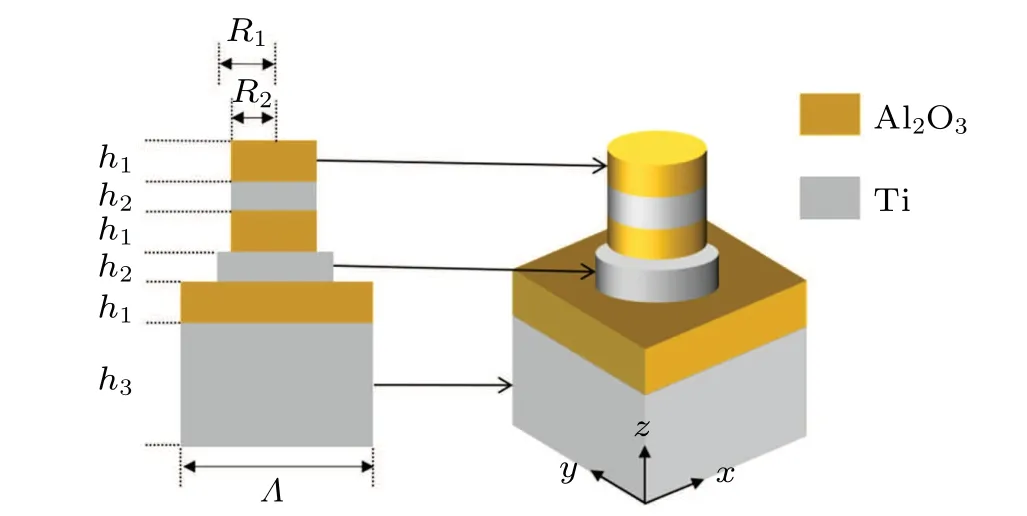
Fig. 1. (a)-(b) Schematic diagrams of designed absorber, with parameters Λ =210 nm,h1=120 nm,h2=30 nm,R1=100 nm,and R2=90 nm.
In the simulation, the finite difference time domain(FDTD)method is used to analyze the absorption performance of the absorber. The boundary conditions of the region along thexandyaxes are periodic, and the distance from the left to the right boundary is accurately equal to one period. The perfectly matched layer(PML)is used in thezdirection. The incident wave is of TM polarization(where the electric field is along thexaxis) at normal incidence. Moreover, the BFAST plane wave is employed for oblique incidence. The mesh size is 5 nm×5 nm×5 nm in thex,y,andzdirections,respectively.
The sample structure is fabricated by the magnetron sputtering technique[17]and the electron beam lithography.[18]Firstly, Ti and Al2O3films can be fabricated by sputtering the related materials on the silica substrates in turn. Secondly, a layer of photoresist will be coated on the films and etched by the electron beam lithography to form periodic nanodisks. Thirdly, the Ti nanodisks can be fabricated by successively sputtering Ti on the photoresist strip array. The remained photoresist is removed by the lift-off method. Lastly,steps 2 through 4 above are repeated while sputtering Ti or Al2O3films as the corresponding layer,and it is noted thatR2is smaller thanR1, which means different periods during the lithography process. At this point,the sample is thus formed.
3. Absorption performance analysis
Based on the optimized geometric structure, figure 2 shows the absorption spectra of differently designed absorbers.They are the absorption spectra of the designed structure(black), designed similar structure (blue) withR1=R2=100 nm, and six-layer metal-insulator film stacks (purple),respectively. Obviously, for the designed structure, the absorptivity of the absorber, above 90% can be achieved in a wavelength range of 600 nm-4000 nm, which indicates an ultra-broad bandwidth of 3400 nm. The average absorptivity is calculated fromA=∫λ1λ2A(λ)dλ/(λ1-λ2),[19]whereλ1is 4000 nm andλ2is 600 nm. According to the formula,the average absorptivity in this wavelength range can reach 91.5%.Moreover, it has extremely high absorption (R >99%) in a range from 631.97 nm to 835.06 nm and from 988.99 nm to 1120.10 nm. Additionally, the relative absorption bandwidth(RAB)can describe the absorption performance,which is defined as RAB=2(λmax-λmin)/(λmax+λmin),whereλmaxandλminare the larger and smaller wavelengths in a wavelength region with absorptivity higher than 90%. Based on the above formula,the RAB value is obtained to be 147.8%.
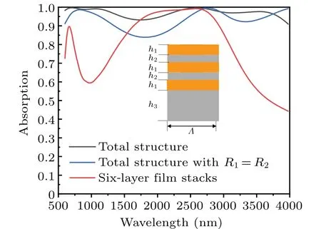
Fig. 2. Absorption performances of total structure (black), total structure with R1 =R2 =100 nm (blue), and six-layer metal-insulator film stacks(red).
Then,for comparison,we analyze the absorption of a similar structure(blue)withR1=R2=100 nm. It is clear that the broadband absorption spectrum with absorption less than 90%ranges from 1339.06 nm to 2295.28 nm, which narrows the bandwidth(A >90%)within the analyzed range.However,the absorptivity of the six-layer metal-insulator film stacks (red)is larger than 90%in a wavelength range from 1639.31 nm to 2904.82 nm,whose corresponding bandwidth is 1265.51 nm,which is narrower than the designed structure bandwidth of 3400 nm. It can be seen from Fig. 2 that the bandwidth is narrowed due to the absorption valley at 969.96 nm. In Table 1, we find that the proposed structure achieves a broader bandwidth and better absorption performance with fewer layers than other absorbers based on cascaded nanodisk arrays.
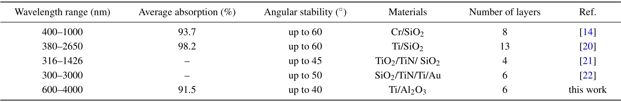
Table 1. Comparison among proposed structures with other relevant absorbers.
To illustrate the physical mechanism of ultra-broadband absorber, the distributions of the electric and magnetic field at the positions of four absorption peaks (λ= 697.93 nm,λ=1059.54 nm,λ=2516.31 nm,andλ=3538.57 nm)are analyzed. Figures 3(a) and 3(b) show the electric and magnetic field distributions at 697.93 nm under TM polarization,respectively. The white lines represent the outline of the structure and show two periods. The results in Fig. 3 show that the enhancement of the electric field dominates the broadband absorption. In Fig. 3(a), the enhanced electric field concentrates mainly in the gap of the top Ti nanodisks, especially near the upper,lower,left,and right edges of the Ti nanodisks.The electric field distribution indicates the appearing of the plasmonic resonant cavity(PRC)mode[23,24]generated by the gap between adjacent Ti nanodisks, as well as the excitation and near-field coupling of the local surface plasmons (LSPs)of the metal Ti nanodisks.[25-27]In Fig. 3(b), the normalized magnetic field distribution shows that the excitation of PSP is evident in the top Al2O3nanodisks,[28,29]while the PSP simultaneously propagates into the middle Al2O3nanodisks.As shown in Figs. 3(b), 3(d), 3(f), and 3(h), it can be seen that the PSP gradually propagates into the middle Al2O3nanodisks and Ti substrate with the increase of resonance wavelength. Therefore,the incident light is coupled to the Al2O3-Ti-Al2O3nanodisk array via the excited plasmon resonant cavity (PRC) and LSPs, and then excites PSPs of the bottom Ti nanodisk and the Al2O3-Ti film layer. All in all, the PRC mode and LSPs are responsible for the high absorption, and the excited PSPs further enhance the light absorption.[25]
In Figs.3(c),3(e),and 3(f),the difference from Fig.3(a)lies in the fact that the enhanced electric field is mainly located in the gap of the bottom Ti nanodisks, and especially near the upper,lower,left,and right edges of the Ti nanodisks.This phenomenon can be explained by the fact that the size of the top Ti nanodisk is smaller than that of the bottom Ti nanodisk. The nanodisks with different sizes will interact with the light at different wavelengths.[30]That is, at a longer wavelength,the absorption of the structure comes mainly from the bottom Ti nanodisk. Besides,when the resonance wavelength changes from 697.93 nm to 3538.57 nm,the electric field becomes stronger, indicating that the resonance of the hybrid is enhanced.
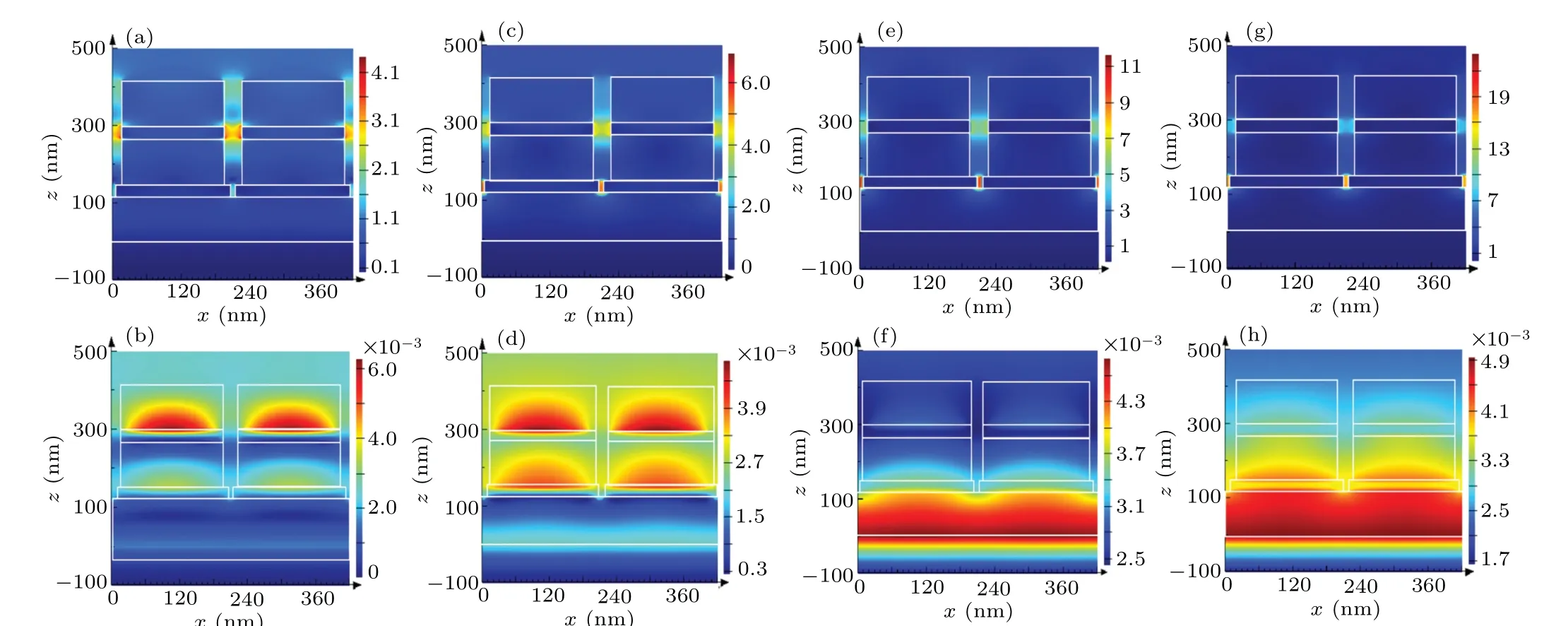
Fig.3. Distributions of electric and magnetic field at four resonance absorption peaks in x-z plane when y=105 nm. The parameters are the same as those in Fig.1. Panels(a),(c),(e),and(g)for electric field distributions;(b),(d),(f),and(h)for the magnetic field distributions at λ =697.93 nm,λ =1059.54 nm,λ =2516.31 nm,and λ =3538.57 nm,respectively. White lines represent the outline of the structure and show two periods.
We further analyze the broadband perfect absorption by using the impedance matching method,[31]which plays an extremely crucial role in perfect absorbers. Using effective medium theory to analyze impedance matching condition,the relationship between impedanceZandSparameter can be described by[32,33]
whereS11,S21,S12,andS22areSparameters,S11andS21are the reflection coefficient and transmission coefficient of the entire structure,respectively,andn,k,anddare effective refractive index, wave vector, and total thickness of the structure,respectively,andd=h1+h2+h1+h2+h1+h3.
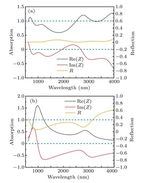
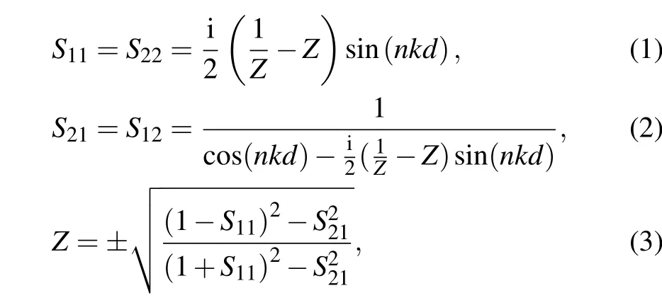
Fig. 4. Curves of absorption and reflection versus wavelength for (a) designed structure and(b)six-layer metal-insulator film stacks.
Figures 4(a)and 4(b)exhibit the impedance and reflection of the structure and corresponding six-layer metal-insulator film stacks,respectively. The parameters are the same as those in Fig. 2. Obviously, comparing with the six-layer metalinsulator film stacks, the real part ofZof our designed structure is close to 1,the imaginary part is close to 0,andRis close to 0 at the working wavelength. The structural impedance better matches with the free space impedance (Z0=1), thus reducing the structural reflection and resulting in a perfect broadband absorption.
4. Results and discussion
To evaluate the influence of structural parameters on the absorption performances, the curves of absorption spectraversus R2are indicated in Fig.5(a). The radiusR2of the upper Al2O3-Ti-Al2O3nanodisk array changes from 80 nm to 100 nm, and other parameters remain unchanged. WhenR2is only 80 nm, the LSPs have weak near-field couplings, and the absorption bandwidth (A >90%) is narrow. In addition,in the band wavelengths of 1320 nm-2084 nm and 3047 nm-3719 nm,the absorption gradually decreases withR2increasing.Especially,in the band wavelengths of 1320 nm-2084 nm,two absorption dips(A <90%)are observed asR2increases to 95 nm. WhenR2continues to increase to 100 nm,the absorption in this range is below 85%.It is because light coupled into the Al2O3-Ti-Al2O3nanodisk array by the PRC and LSPs can excite only the PSPs near the top Ti nanodisk. Partial energy is reflected into the top air by the Ti nanodisk, resulting in reduced absorption. Interestingly, the increasedR2leads the near-field coupling of LSPs to be enhanced,[34]which gives rise to the redshift of the resonance band and the increase of absorption in the long-wavelength region(i.e., the broadened absorption band). These excellent characteristics are essential for absorption devices in industrial applications.
From Fig.5(b),we can see the curves of absorption spectra verseR1andR2,fixingR1-R2=10 nm.WhenR1increases from 80 nm to 100 nm,R2increases from 70 nm to 90 nm accordingly. It can be clearly observed that the bandwidth(A >90%)has a relatively large change,that is,the bandwidth and the average absorptivity continue to increase withR1andR2increasing.The above analysis shows that with the increase ofR1andR2,light coupled to the Al2O3-Ti-Al2O3nanodisk array by PRC and LSPs can excite the PSPs near the top and bottom Ti nanodisks, and the near-field coupling of LSPs is enhanced,thereby improving the absorption performance.[34]
Furthermore, we investigate the absorption performance when the thickness of each layer changes. In Fig. 6(a), the thickness of the top Al2O3nanodisk array changes from 60 nm to 180 nm. The average absorption increases with the thickness increasing. Also, we can see from Fig. 6(b) that the absorption decreases in the shorter wavelength and from Fig.6(c)that the absorption increases in the longer wavelength for the increased thickness of the bottom Al2O3nanodisk array. Additionally,as the thickness of bottom Al2O3film increases,the bandwidth (A >90%) is broadened but the absorption is less than 90%when the thickness is equal to 180 nm.
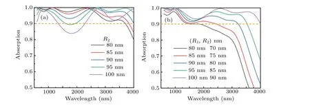
Fig.5. Curves of(a)absorption versus wavelength for different values of R2 and(b)absorption versus wavelength for different values of R1 and R2,while R1-R2=10 nm.
Fig.6. Curves of absorption versus wavelength for(a)top-Al2O3 layer,(b)middle-Al2O3 layer,and(c)bottom-Al2O3 layer for different thickness values.
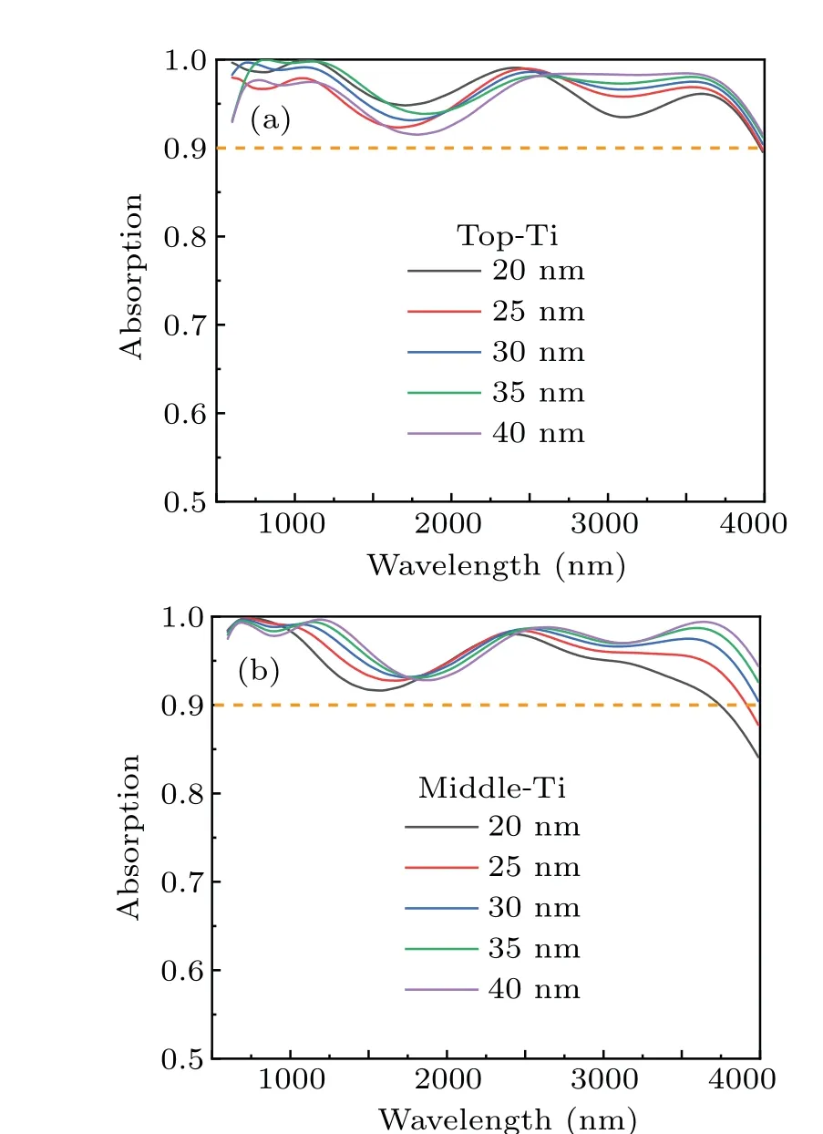
Fig. 7. Curves of (a) absorption spectra versus wavelength of top-Ti layer and(b)middle-Ti layer for different thickness values.
As shown in Fig.7(a),the thickness of the top Ti nanodisk array changes from 20 nm to 40 nm,the absorption bandwidth(A >90%) is relatively unchanged. However, in Fig. 7(b),it narrows with the thickness of middle Ti nanodisk array increasing, which is due to the weaker near-field coupling of LSPs. Moreover,because the thickness of the bottom Ti substrate is thick enough to ensure that the transmission is nearly zero,we do not discuss the influence of the thickness.
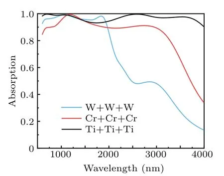
Fig.8.Curves of absorption versus wavelength for different metal materials.
The influence of metal material on the absorption performance of the absorber is also considered in Fig. 8. The Ti layer is replaced by Cr or W, and the dielectric constants of Cr and W are obtained from Palik’s data.[16]The results can imply that when using W, although a relatively narrow band is performed in a range of 600 nm-1968.65 nm(1368.65 nm in span,A >90%), it is comparable to those obtained in the metal-insulator multilayer film stacks.[35,36]The difference observed here is determined by the intrinsic dispersion characteristics of the metal. The lossy metal, Ti or Cr with an appropriate thickness satisfies the impedance matching conditions,to provide a plasmon cavity with a low quality factor in an ultra-wideband wavelength range.[37,38]
Figure 9(a)shows the absorption spectra as a function of polarization angle, where 0°represents the TM polarization and 90°refers to the TE polarization. Obviously, when the polarization angle increases from 0°to 90°,the broadband absorption(above 90%)in a wide wavelength range of 600 nm-4000 nm almost remains unchanged. This indicates the polarization independence of the ultra-wideband absorber.
Finally,we perform calculations to verify the angular dependence of TM and TE polarization,and the results are illustrated in Figs.9(b)and 9(c). The incident angle of light varies from 0°to 40°, the absorption bandwidth (A >90%) under TM polarization or TE polarization remains almost the same as the absorption bandwidth in the case of normal incidence.Overall, this absorber is observed to possess high absorption at an oblique incident angle.
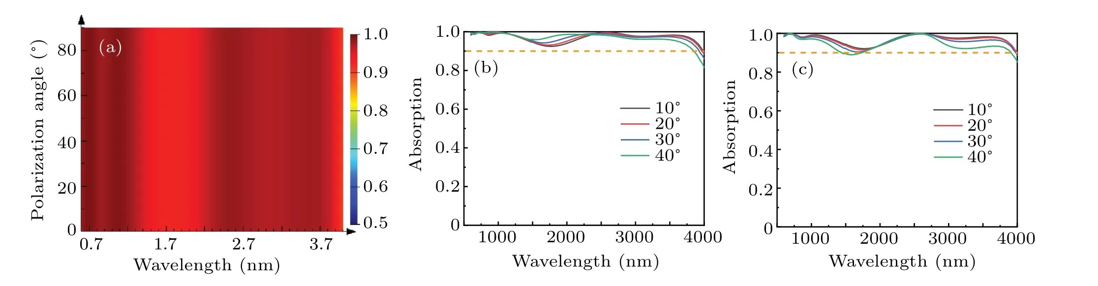
Fig.9. (a)Polarization angle versus wavelength,and curves of absorption versus wavelength for different incident angles under(b)TM polarization and(c)TE polarization.
5. Conclusions
We demonstrated an ultra-broadband and polarizationindependent absorber based on cascaded nanodisk arrays by using the FDTD method, which can reach up to 3400 nm(R >90%)in a wavelength range of 600 nm-4000 nm.Specifically,the absorption peak is 99.99%,and the average absorptivity is 91.5%with an RAB of 147.8%. The physical mechanism for the proposed absorber results from the synergistic effect of the LSPs,PRC modes,and PSPs. Moreover,based on the impedance theory,the impedance of the structure matches better with the impedance of the free space than that of the sixlayer metal-insulator film stacks in this analyzed wavelength range. Furthermore,the absorber exhibits a remarkable tolerance for incident angle and polarization angle of the incident light. This design may provide an alternative scheme towards ultra-broadband absorption and be applied to the area of photoelectric detection and optical imaging.
Acknowledgement
Project supported by the National Natural Science Foundation of China(Grant Nos.61775140 and 62005165).

- Chinese Physics B的其它文章
- Helium bubble formation and evolution in NiMo-Y2O3 alloy under He ion irradiation
- Dynamics and intermittent stochastic stabilization of a rumor spreading model with guidance mechanism in heterogeneous network
- Spectroscopy and scattering matrices with nitrogen atom:Rydberg states and optical oscillator strengths
- Low-overhead fault-tolerant error correction scheme based on quantum stabilizer codes
- Transmembrane transport of multicomponent liposome-nanoparticles into giant vesicles
- Molecular dynamics simulations of A-DNA in bivalent metal ions salt solution