Blue phosphorene/MoSi2N4 van der Waals type-II heterostructure:Highly efficient bifunctional materials for photocatalytics and photovoltaics
2023-03-13 09:19:46XiaohuaLi李曉華BaojiWang王寶基andSanhuangKe柯三黃
Chinese Physics B 2023年2期
Xiaohua Li(李曉華) Baoji Wang(王寶基) and Sanhuang Ke(柯三黃)
1School of Physics and Electronic Information Engineering,Henan Polytechnic University,Jiaozuo 454000,China
2MOE Key Laboratory of Microstructured Materials,School of Physics Science and Engineering,Tongji University,Shanghai 200092,China
Keywords: ab initio study,heterostructure,photovoltaic cell,photocatalytic water splitting
1.Introduction
Semiconductor photocatalysts have received much attention in recent years due to their great potentials for the development of clean energy technologies, as well as for environmental protection and remediation.[1-3]Specifically,two-dimensional(2D)materials are considered excellent candidates for solar cell and water-splitting photocatalyst because of their high specific surface areas and short migration path to the reaction surface for photoexcited electron-hole pairs.[4,5]Currently, a series of 2D materials such as transition metal carbides or nitrides,[6-9]transition-metal dichalcogenides(TMDs)[10,11]have been found to have great potential for photovoltaic and/or water-splitting applications.However,it is found that a pure semiconductor often cannot meet the requirements of practical applications.For example,the photogenerated carriers in such materials are not well separated spatially,which can lead to a fast electron-hole recombination and thus reduce the solar energy conversion.Fortunately, it is evident that establishing the 2D van der Waals heterostructure (vdWH) with the type-II band structure is a fascinating approach to conquer this challenge,where photoexcited electrons and holes are distributed separately in the two materials,thus prolonging carrier lifetime.[12,13]Typically,there are two major strategies regarding the construction of the 2D vd-WHs: the top-down approach and bottom-up approach.[14]It is heartening to note that so far large amounts of 2D vd-WHs are successfully constructed experimentally,[15,16]which makes their practical application possible in the future.
Recently,2D layered phosphorus,which is a new member of the family of 2D materials,have gathered a great deal of attention due to their fascinating properties.Note that the carrier mobility of black phosphorene(BlackP)is 1000 cm2·V-1·s-1at room temperature[17]which is considerably higher than that of a value 200 cm2·V-1·s-1obtained by 2D layered TMDs.As an allotrope of BlackP, blue phosphorene (BlueP) has been successfully synthesized through molecular beam epitaxial growth on a Au (111) substrate by using the BlackP as a precursor.[18]Theoretical calculations indicate that the BlueP has a wider indirect gap and a higher hole mobility(1700 cm2·V-1·s-1)than that of BlackP.[19]Appropriate band edge alignments make it suitable for water splitting although it may suffer from low efficiency in separating photogenerated carriers.[13]And its photocatalytic properties can be modified by applying external strains or modulating layer numbers.[20]These properties make it a potential material for field effect transistors and other 2D electronic devices.Of course, we also note that both BlackP and BlueP have weak structural stability at ambient conditions in the presence of water and oxygen molecules.[21]The multilayer BlackP or BlueP is predicted to have better stability than its single layer due to the enhanced interlayer coupling and screening.[20,22]In this sense,constructing 2D BlueP-based vdWH can be considered to protect it from ambient degradation.So far, a large number of BlueP-based heterostructures have been studied.Our upfront works showed that BlueP/BSe and BlueP/Mg(OH)2vdWHs possess significant potency for water splitting reactions.[12,13]BlueP/Sc2CX2(X=O, F)vdWHs have great potential in the field of photocatalysis and photovoltaics.[23]The work of Gaoet al.showed that BlueP/g-GeC is a promising candidate for photocatalytic water splitting.[24]In short, BlueP is an excellent material to establish 2D vdWH with the high-efficiency photovoltaic and photocatalytic properties.
Recently, a new 2D layered material, MoSi2N4, has been successfully synthesized using the chemical vapor deposition (CVD) method.[6]Experimental results indicate that it has semiconducting characteristic (bandgap~1.94 eV)with good mechanical strength and air-stability.Motivated by the exciting properties of MoSi2N4, many efforts have been dedicated to revealing its novel properties and potential applications.[7,8,25]Specifically, MoSi2N4monolayer owns high electron and hole mobilities, strong visible light absorption and suitable band edge positions for photocatalytic water splitting.[7,25]Similarly, the exotic properties of MoSi2N4monolayer can be further tuned by combining with other 2D materials.To date,various MoSi2N4-based vdWHs have been investigated because they possess multitudinous new phenomena and unique properties.[26]For instance,Zenget al.demonstrated that MoSi2N4can be coupled with C2N to form a typical type-II heterostructure with thermodynamic stability.[26]And this heterostructure is found to be a very promising photocatalyst for hydrogen production.Based on the aforementioned data,we reasonably speculate that the BlueP/MoSi2N4vdWH may be a promising bifunctional materials and holds great potential to be synthesized in experiments.
In this work, we focus on the study of BlueP/MoSi2N4vdWH as potential photocatalytic or photovoltaic materials.Its geometric structure,electronic structure,optical properties,and band edge,etc.are explored by performing first-principles calculations.The results show that BlueP/MoSi2N4vdWH is a semiconductor with type-II band structure, which is conducive to the efficient separation of the photoexcited electronhole pairs.Stronger optical absorption in the visible-UV light region is found compared with its components,along with the high solar-to-hydrogen(STH)and power conversion(PC)efficiencies,predicting its substantial potential in the field of solar energy utilization.
2.Methods
The density-functional theory(DFT)calculations are carried out by employing the Viennaab initiosimulation package (VASP)[27]with the projected augmented wave (PAW)method.[28]The DFT-D2 level[29]is adopted for the longrange vdW interaction.During structural optimization, the Perdew-Burke-Ernzerhof (PBE) functional and generalized gradient approximation(GGA)are used to calculate the electron exchange and correlation.[28]Dipole correction is employed to cancel the errors of electrostatic potential.[30,31]The cut-off energy is set to 500 eV.The thickness of the vacuum layer is set to 40 °A.The convergence criteria for the forces and energy are set to 0.01 eV/°A and 10-5eV, respectively.The Heyd-Scuseria-Ernzerhof hybrid functional(HSE06)[32,33]is applied to obtain the precise electronic structures and optical properties.The 21×21×1 and 9×9×1k-point meshes are used for PBE and HSE06 calculations, respectively.And in the HSE06 method, we adopt the mixing parameter of 0.125 and the screen factor of 0.20 °A-1to obtain a band gap close to the experimental value.
3.Results and discussion
The crystal structures of BlueP and MoSi2N4monolayers are displayed in Figs.1(a)and 1(c),respectively.The optimized lattice parameters of BlueP and MoSi2N4monolayers are 3.27 °A and 2.91 °A, respectively, which in accordance with the previous predicted values.[6,19]The band structures of BlueP and MoSi2N4monolayers are given in Figs.1(b)and 1(d), respectively.Obviously, both BlueP and MoSi2N4monolayers are indirect band gap semiconductors.For BlueP monolayer, its conduction band minimum(CBM)locates between theΓandMpoints while the valence band maximum(VBM) locates between theKandΓpoints.Its band gap is 2.35 eV using modified HSE06, which is closed to the previously reported data.[18,23]For the MoSi2N4monolayer, its VBM and CBM are located at theΓand theKpoint,respectively.The calculated band gap (2.06 eV) matches with experimental band gap of 1.94 eV.[6]We further note that polarization and spin-orbit coupling(SOC)effect have very small effects on the band dispersion for both the BlueP and MoSi2N4monolayers(see Fig.A1).So we will neglect those effects in the following sections.
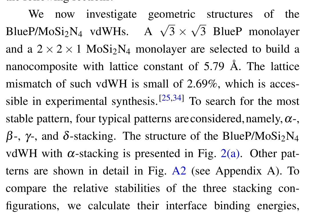


Fig.1.Top and side views of the (a) BlueP and (c) MoSi2N4 monolayers.The violet rhombus indicates the primitive unit cell.The band structures given by the modified HSE06 for the(b)BlueP and(d)MoSi2N4 monolayers.

Fig.2.(a) Top view (upper panel) and side view (down panel) of the BlueP/MoSi2N4 vdWH with α-stacking.The supercell boundary is denoted by violet rhombus.The optimized interlayer distance d is indicated.(b)The projected band structures of BlueP/MoSi2N4 vdWH using modified HSE06 calculation,in which the different colored spheres indicate the contributions from the different components.The corresponding total and partial density of states of the heterostructure are given in their right panels.
The projected band structure of theα-stacking BlueP/MoSi2N4vdWH calculated by the amended HSE06 is illustrated in Fig.2(b).Clearly, the VBM and CBM of the BlueP/MoSi2N4vdWH locate atΓpoint andKpoint,respectively, resulting in the feature of the indirect band gap.The calculated HSE06 band gap is predicted to be 1.67 eV,which satisfies the demands of water splitting(≥1.23 eV)and fulfills the needs for efficient sunlight utilization(1.55 eV-3 eV).[35]Furthermore, the CBM is mainly contributed by the BlueP monolayer, while the VBM is dominated by the MoSi2N4sublayer,which can be further confirmed from the partial density of states (PDOS) as shown in Fig.2(b) (right panel).It can be found that the CBM mainly stems from the p states of P atoms, while the VBM state is mainly dominated by the d states of the Mo atoms.Hence, this vdWH has a type-II band alignment,which will spontaneously separate photogenerated electrons and holes, so as to achieve high efficiency solar energy conversion.
The interlayer interaction in the BlueP/MoSi2N4vdWH will induce the charge transfer between two individuals,which can be analyzed by the charge density difference(Δρ(z))along thezdirection.Δρ(z)can be determined by
whereρH(z),ρB(z), andρM(z) represent the charge densities of the BlueP/MoSi2N4vdWH,the pristine BlueP and the MoSi2N4monolayers, respectively.As shown in Fig.3(a),some charges are transferred from the MoSi2N4sheet to the BlueP layer.The amount of transferred electrons up tozpoint is determined by
The righty-axis of Fig.3(a)unveils that about 0.61 electrons per unit cell is transferred from the MoSi2N4layer to the BlueP sheet,which is calculated by the value of ΔQ(z)at the BlueP/MoSi2N4interface.[36]The charge transfer induces an intrinsic built-in electric field(Ein)with its direction pointing from MoSi2N4layer to BlueP layer,which can extend the recombination lifetime of the electron-hole pair.Moreover,the interface dipole momentμ(z)is also calculated by[37]
Obviously, an inward pointing dipole is formed in the interface(see Fig.3(b)).[37]That is to say,it points in the opposite direction ofEin, which will further suppress the recombination of photogenerated electrons and holes and prolong their life-span.

Fig.3.(a) Plane-averaged charge density difference Δρ (gray line),the amount of transferred charge ΔQ (magenta line) and (b) interfacial dipole momentμ (blue line)along the normal direction of the heterostructure.The inset in(a)is the 3D isosurface of the charge density difference.The yellow and cyan areas represent electrons accumulation and depletion, respectively.The vertical dashed line denotes the BlueP/MoSi2N4 vdWH interface.
As mentioned above, the BlueP/MoSi2N4vdWH has great potential as visible light photocatalyst.In order to evaluate its feasibility for water splitting, we align the band edge positions of heterostructure to the vacuum levels.As shown in Fig.4(a),the band edges of the BlueP/MoSi2N4vdWH can perfectly straddle the water redox potential at pH=0, that is,the BlueP/MoSi2N4vdWH can effectively promote the water splitting reaction due to the positive oxidation potential of VBM and the negative reduction potential of CBM.Besides,as we all know, the conduction band offset (CBO, ΔEc) and valence band offset(VBO,ΔEv)are crucial factors that affect the photocatalytic performance of the BlueP/MoSi2N4vdWH.Here, the calculated ΔEcand ΔEvare around 0.82 eV and 0.29 eV,respectively.

Fig.4.(a) The band edge positions of the BlueP/MoSi2N4 vdWH are calculated within the HSE06 level.For comparison,the redox potentials of water splitting at pH=0 are shown.(b)The optical absorption spectra A(ω) of BlueP, MoSi2N4 monolayers and BlueP/MoSi2N4 vdWH are also calculated based on HSE06 functional.
Moreover,we evaluate the STH efficiency(ηSTH)of photocatalytic water splitting for BlueP/MoSi2N4heterostructure as follows:[38]
whereP(hω) is the AM 1.5 solar energy flux at the photon energy ofhω,Eis the energy of photons that can actually be used for water splitting.[38-40]As a result, theηSTHof the BlueP/MoSi2N4vdWH achieves 15.8%, which is economically viable as water-splitting photocatalyst.[38]
Besides,strong light absorption is also an important factor for solar applications.The absorption spectra of the BlueP/MoSi2N4vdWH and the corresponding isolated layers are calculated and displayed in Fig.4(b).The computational details have been fully described in our previous works.[12,13]Fascinatingly, the designed heterostructure shows more pronounced optical absorption in both visible and UV light region compared with the constituent monolayers, which suggests that the BlueP/MoSi2N4vdWH has great potential as an efficient solar light absorber material.
We further estimate the maximum power conversion efficiencies(ηPCE)of the BlueP/MoSi2N4heterostructure as photovoltaic solar cells by using the Scharber’s method,[41]which is defined as follows:
whereEdgand ΔEcare the donor band gap and conduction band offset,respectively.J(ˉhω)represents the AM 1.5 solar energy flux at the value ofˉhωfor photon energy.The calculatedηPCEvalue is about 10.61%,as marked in Fig.5.And itsηPCEcan be further enhanced by strain engineering (see later discussion).The results indicate that the BlueP/MoSi2N4vdWH can also be a promising photovoltaic material.

Fig.5.Power conversion efficiency contour.The spheres on the contour represent the efficiency limits of the BlueP/MoSi2N4 heterostructures under the different strains.The ηPCE value of the 2L-P/M heterostructure is also labeled.
Next, we will explore the effect of strain on the photocatalytic and photovoltaic properties of the BlueP/MoSi2N4vdWH.Here, the applied in-layer biaxial strainεis defined byε=(a-a0)/a0×100%,whereaanda0represent the lattice constants for the strained and unstrained structures, respectively.Meanwhile,the strain energy per atom is also calculated as followsEs=(Estrained-Eunstrained)/n, wherenis the number of atoms in the unit cell.As shown in Fig.6(a),when the compressive strain decreases from-8% to-4%,the band gap increases gradually and reaches its maximum value (~2.22 eV) atε=-4%.When the strain varies from-4% to +8%, its band gap decreases monotonically.From Fig.6(a)(righty-axis),we also find that the strain energy curve is smooth as a quadratic function under the biaxial strain, indicating that all the strains considered are within the elastic limit.

Fig.6.(a)Calculated band gap and strain energy,and(b)the band-edge positions of the BlueP/MoSi2N4 vdWH under different biaxial strains by the HSE06 functional.The standard redox potentials of water splitting(at pH=0)are denoted by the dashed line.
The band edge positions of the BlueP/MoSi2N4vdWH under different biaxial strain are plotted in Fig.6(b).Obviously, under compression-to-tension strains, the VBM and CBM of BlueP layer remain nearly constant, while the VBM(CBM) of MoSi2N4layer moves up (down).As a result,the greater compressive or tensile strains induce a transition from type-II to type-I band alignment,which is detrimental to photocatalysis.[42]However,the type-II band alignment properties are maintained under a moderate strain (-2%≤ε ≤+4%).In particular,whenε=-2%,its CBM and VBM overpotentials are all closed to 0.4 eV,which is adequate for H2/O2production from water.Besides,we note that the tensile strain effectively reduces theEdgand ΔEc,thus significantly improving theηPCE.AηPCEas high as~21.20% can be achieved under the 4% tensile strain, as marked in Fig.5.Hence, the tensile strain is an effective way to enhance theηPCEof the BlueP/MoSi2N4vdWH.
Finally, we will focus on the effect of multilayer BlueP on the electronic properties of the MoSi2N4-based vdWHs.Here, we consider two cases: bilayer BlueP/MoSi2N4(2LP/M) and trilayer BlueP/MoSi2N4(3L-P/M) heteromultilayers,as illustrated in Figs.7(a)and 7(c),respectively.The multilayer BlueP adopts the stable AA-stacking configurations.[20]The band structures are shown in Figs.7(b)and 7(d),respectively.As can be seen, the heteromultilayers are all indirect semiconductors and the band gaps decrease with the increase of the thickness owing to the quantum confinement effect.The 2L-P/M heterostructure forms a type-II alignment, similar to heterobilayers, whereas the 3L-P/M heterostructure forms a type-I alignment, which implies that altering the number of constituent layers can lead to the transition from type-II to I.In the meantime,we find that the 2L-P/M heterostructure is also a promising water splitting material with a practicalηSTHvalue(~15.6%).Unfortunately, the multilayer BlueP dramatically increases the ΔEc,thus significantly decreasing theηPCE.The calculatedηPCEvalue of 2L-P/M heterostructure is only 3.2%,as marked in Fig.5.For 3L-P/M heterostructure,type-I band alignment and inappropriate band edge positions make it unsuitable for water splitting or photovoltaic solar cells.
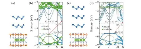
Fig.7.Side views of(a)2L-P/M and(c)3L-P/M heterostructures.Projected band structures with modified HSE06 functional of(b)2L-P/M and(d)3L-P/M heterostructures,referring to the vacuum level.The redox potentials(dashed line)of water splitting are shown for comparison.
4.Conclusion
In this paper, we have investigated the electronic,optical, photocatalytic and photovoltaic properties of the BlueP/MoSi2N4vdWH based on the first principles calculations.Our findings indicate that BlueP/MoSi2N4vdWH is an indirect-band-gap semiconducting material with type-II band alignment.With the combination of suitable band gaps,proper bandedge positions, effective separation of carriers and high STH efficiency, the BlueP/MoSi2N4vdWH shows great possibility to be used as photocatalysts for water splitting.Compared with its composing BlueP and MoSi2N4monolayers,the heterostructure exhibits more efficient optical absorption.Also, the BlueP/MoSi2N4vdWH is found to have potential for application in photovoltaic cell.Further investigations reveal that its photocatalytic and photovoltaic properties can be significantly modulated by external uniform strains.Especially,a 4%strain will increase itsηPCEby about 99.9%.The layer-dependent behavior of the BlueP/MoSi2N4vdWH is also studied.All these data strongly suggest that BlueP/MoSi2N4vdWH is a very promising photocatalytic and photovoltaic material.
Appendix A

Fig.A1.The calculated band structures of (a) BlueP and (b) MoSi2N4 monolayers by considering spin polarization.Band structures of (c)BlueP and(d)MoSi2N4 monolayers with and without spin-orbit coupling(SOC)effect.The results are from the vdW-DFT/PBE calculations.
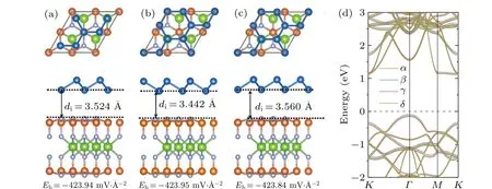
Fig.A2.Top (upper panel) and side (lower panel) views of the BlueP/MoSi2N4 heterostructures with different stacking sequences: (a) βstacking,(b)γ-stacking,and(c)δ-stacking.The corresponding interlayer distances(di)and binding energies(Eb)are also labeled.(d)Band structures of the BlueP/MoSi2N4 heterostructures with α-,β-,γ-and δ-stacking given by the PBE functional.
Acknowledgements
Project supported by the National Natural Science Foundation of China (Grant No.11374226), the Fundamental Research Funds for the Universities of Henan Province of China(Grant No.NSFRF200331),the Foundation of Henan Educational Committee (Grant No.20A140013), as well as by the High-performance Grid Computing Platform of Henan Polytechnic University.
- Chinese Physics B的其它文章
- Analysis of cut vertex in the control of complex networks
- Atlas of dynamic spectra of fast radio burst FRB 20201124A
- Investigating the characteristic delay time in the leader-follower behavior in children single-file movement
- Micro-mechanism study of the effect of Cd-free buffer layers ZnXO(X =Mg/Sn)on the performance of flexible Cu2ZnSn(S,Se)4 solar cell
- Thermally enhanced photoluminescence and temperature sensing properties of Sc2W3O12:Eu3+phosphors
- Heterogeneous hydration patterns of G-quadruplex DNA