Novel GaN-based double-channel p-heterostructure field-effect transistors with a p-GaN insertion layer
2023-11-02 08:12:52XueruiNiu牛雪銳BinHou侯斌MengZhang張濛LingYang楊凌MeiWu武玫XinchuangZhang張新創(chuàng)FuchunJia賈富春ChongWang王沖XiaohuaMa馬曉華andYueHao郝躍
Chinese Physics B 2023年10期
Xuerui Niu(牛雪銳), Bin Hou(侯斌),?, Meng Zhang(張濛), Ling Yang(楊凌),?, Mei Wu(武玫),Xinchuang Zhang(張新創(chuàng)), Fuchun Jia(賈富春), Chong Wang(王沖), Xiaohua Ma(馬曉華), and Yue Hao(郝躍)
1Key Laboratory of Wide Band-Gap Semiconductor Materials and Devices,School of Microelectronics,Xidian University,Xi’an 710071,China
2School of Advanced Materials and Nanotechnology,Xidian University,Xi’an 710071,China
Keywords: GaN, double-channel heterostructure field-effect transistors, p-GaN insertion layer, C-doped buffer layer
1.Introduction
In recent years, GaN has demonstrated great prospects in the field of power electronics due to its wide bandgap and high electron mobility.GaN-based high electron mobility transistors (HEMTs) on Si substrates have been widely explored in research, and fabricated as power switches with a high breakdown voltage for commercial usage.[1,2]The application of discrete GaN-based power switches requires the collaboration of Si-based peripheral circuit structures such as gate driver,controller and protection modules.However,the differences between the two materials and the interconnections between devices can introduce extra parasitic effects to the power conversion circuit, which induce instability of GaN power switches and circuits.[3-5]Furthermore, the high-temperature stability of Si is worse than that of GaN.These problems deteriorate the performance of GaN-based HEMTs and have seriously hindered the industrialization process.
GaN-based monolithic integration technology is an emerging but promising solution to solve these problems; it not only allows GaN-based devices to have more functions but also enhances circuit robustness and promotes the miniaturization of the power conversion system.[6,7]Therefore, there has been great interest in researching the integration of GaNbased gate drivers and power switches.So far, most of the developed GaN-based gate drivers are based on the combination of enhancement mode (E-mode) and depletion mode(D-mode) n-channel HEMTs (n-HEMTs).But such directcoupled FET logic circuits suffer from serious power losses that are not conducive to the efficiency of the power conversion system.[8,9]Given these considerations, a complementary logic circuit prepared from GaN-based E-mode p-channel heterostructure field-effect transistors(p-HFETs)and E-mode n-HEMTs has been proposed as a promising alternative to greatly suppress power losses.
However,p-HFETs have encountered many challenges in their development.One of the major challenges is the much lower mobility of the holes in GaN than that of the electrons,which will lead to a low on-state current and decreased driving capability of p-HFETs.To address this issue, aggressive lateral scaling of p-HFETs,the fin configuration,[10]GaN/AlN heterostructures[11,12]and multi-channel structures[13,14]have been proposed.The reported multi-channel p-HFETs introduced Mg doping in each layer, but the presence of the large number of Mg impurities in the heterostructure resulted in severe ionized-impurity scattering, which in turn reduced the mobility of the holes.
In this work, we propose a double heterostructure with a p-GaN insertion layer to realize double-channel p-HFETs,where holes can be distributed in two channels.By using Silvaco TCAD simulations,the influences of the thickness of the upper AlGaN layer, the doping impurities and concentrations of the GaN buffer layer,and the thickness and doping concentration of the p-GaN insertion layer on the densities of the twodimensional hole gas (2DHG) and valence band energies of two channels are discussed;this complements the mechanisms concerning the impact of doping on the modulation of energy bands in double heterostructures.The increased 2DHG density in the lower channel and the reduced doping concentration in the GaN buffer layer can be achieved by the insertion of a p-GaN layer between the AlGaN layer and C-doped GaN buffer layer.It is worth noting that the distribution of the 2DHG between the two channels is mainly affected by the variation in the thickness of the upper AlGaN layer.Our results suggest that a double heterostructure with a p-GaN insertion layer is an attractive approach for realizing double-channel p-HFETs.
2.Device structure
The typical cross-sectional structure of a double-channel p-HFET is exhibited in Fig.1(a).The designed epilayer,from top to the bottom, consists of a 20 nm p++-GaN layer (Mg:5×1019cm-3), a 40 nm p-GaN layer (Mg: 1×1019cm-3),a 10 nm upper unintentionally doped(UID)-GaN layer,an upper Al0.25GaN layer,a 10 nm UID-GaN layer,a 20 nm lower Al0.25GaN layer and a 3 μm GaN buffer layer with residual background electrons of 1×1015cm-3.Mg can diffuse from the p-GaN layer to the UID-GaN layer during the growth of the heterostructure, which makes the upper UID-GaN layer into a p-type one.The diffusion coefficient of Mg is set to be 0.2.All the results in this work were obtained using Silvaco TCAD.The model used in these simulations has been calibrated to match the published results.[15]
C doping and Fe doping play a key role in achieving a highly resistive GaN buffer layer,[16,17]which will also influence the energy band and density of the 2DHG in the double heterostructure.C doping in the simulations is modeled as deep acceptor traps with energyEV+0.9 eV,[18]while Fe doping is modeled as acceptor traps with energyEC-0.57 eV.[19]The ionized densities are calculated according to a literature study.[20]The 2DHG density is the integral of hole concentration in the GaN channel layer with respect to its channel thickness.Figures 2(a)and 2(b)show the influence of the C-doping induced acceptor concentration in the GaN buffer layer on the distribution of holes and the variation of the valence band(i.e.,in the access region).As shown in Fig.2(a), the density of the 2DHG in the upper channel is almost unaffected.However, the 2DHG density in the lower channel increases significantly when the concentration rises from 1×1018cm-3to 1×1019cm-3, and even gets close to that of the upper channel when the concentration is between 5×1018cm-3and 1×1019cm-3.As shown in Fig.2(b), the valence band of the GaN buffer layer rises with the increase in C-doping induced acceptor concentration, which explains the significant increase in the 2DHG density in the lower channel when the concentration exceeds 1×1018cm-3.
The effect of Fe doping in the GaN buffer layer on the 2DHG density in the access region of the two channels is now discussed.It can be seen in Fig.3(a)that when the concentration varies from 1×1016cm-3to 1×1019cm-3, the 2DHG density remains constant in the upper channel but changes slightly in the lower one.Figure 3(b)displays the variation of the valence band according to different Fe-doping induced acceptor concentrations.The rise of the valence band for the Fedoped GaN buffer layer is not obvious,suggesting that the Fedoped buffer layer is not preferred for the double heterostructure compared with the C-doped one.
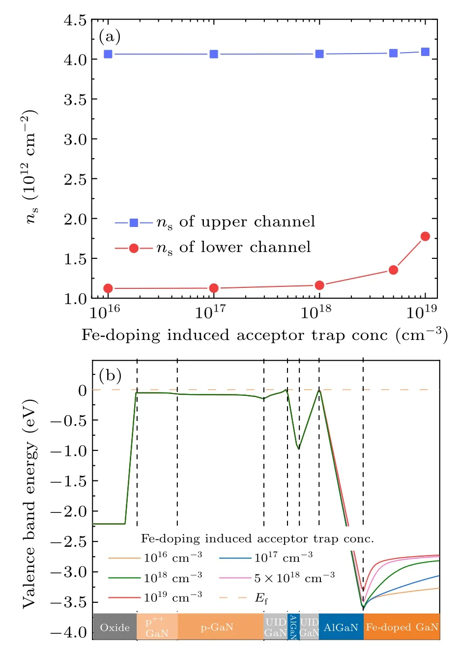
Fig.3.Schematic illustration of(a)the distribution of 2DHG density and(b)the variation of the valence band of two channels in the access region with the Fe-doping induced acceptor trap concentration.
3.Results and discussion
Based on the above results,the buffer layer of the double heterostructure utilized in this work is selected to be C doped.For the structure shown in Fig.1(a), the main way to improve the carrier density of the lower channel is to increase the C-doping induced acceptor concentration in the GaN buffer layer.If the concentration is 1×1019cm-3,the carrier density of the lower channel can increase to 5×1012cm-2.Although a highly C-doped buffer layer facilitates the presence of an increased 2DHG density in the lower channel, it introduces other challenges.On the one hand, a C-doped GaN buffer should be grown at a relatively low temperature to enhance incorporation of C in the GaN layer, so that the buffer layer will have poor structural quality resulting in the degradation of hole mobility.[21]On the other hand, acceptor traps introduced by the high C-doped buffer layer will seriously affect the carriers,which leads to the hot-carrier effect,trapping effect and current collapse.[22,23]Since p-GaN has a low trap concentration[24]and its energy band modulation can enhance the 2DHG density in the lower channel,the introduction of the p-GaN insertion layer can improve device performance and reliability without reducing the carrier density.As a result, the C-doping induced trap concentration can be reduced, and the performance of devices can be improved.
Figure 1(b) demonstrates the proposed double heterostructure with a p-GaN layer inserted between the C-doped buffer layer and the AlGaN layer.Based on this heterostructure,the variation of 2DHG density with different thicknesses of the upper AlGaN layer (t1) is discussed, as shown in Fig.4(a).The thickness of the p-GaN insertion layer was set to be 20 nm, while the Mg-doping concentration was 4×1018cm-3.It can be seen from Fig.4(a) that the distribution of the holes between the two channels is critically influenced byt1.Whent1is small, the density of the 2DHG in the lower channel is larger than that in the upper channel, and vice versa.This is mainly because a largert1will increase the density of the 2DHG at the upper GaN/AlGaN interface and screen the holes at the lower GaN/AlGaN interface.Figure 4(b)shows the effect of differentt1values on the valence band energy.It can be observed that the hole quantum well (QW) only exists in the lower/upper channel whent1=2 nm/13 nm,while hole QWs exist in both channels whent1=6 nm.
During the fabrication process, the p-GaN layer in the gate region requires etching followed by the deposition of a dielectric layer.These two steps will inevitably cause damage and create a high density of interface states in the recessed region,leading to the degradation of carrier mobility and operational stability.[25,26]Hence, a low 2DHG density in the upper channel is preferred.When the AlGaN layer is thinner than 5 nm, the 2DHG density in the lower channel is much higher than that in the upper channel.Nevertheless,this is not conducive to the optimization of performance of p-HFETs.A much higher density of 2DHG in the lower channel will not only affect the off-state characteristics of the devices but also increase the scattering effect between holes.As a result, a 5 nm AlGaN layer is selected in our simulations.
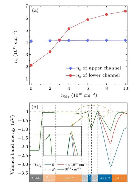
Fig.5.Variation of(a)2DHG density and(b)valence band energy of two channels in the access region with the Mg-doping concentration in p-GaN insertion layer.
The effect of doping concentrationnMgin the p-GaN insertion layer on the density of the 2DHG in the access region was evaluated, as shown in Fig.5(a).The thicknesses of the upper AlGaN layer and p-GaN insertion layer were set to be 5 nm and 20 nm, respectively.It can be observed thatnMgin the p-GaN layer greatly influences the lower channel while demonstrating little impact on the upper one.The larger thenMg,the higher the 2DHG density in the lower channel.WhennMgincreases from 2×1018cm-3to 4×1018cm-3,nsin the lower channel increases significantly.This is mainly a result of the fact that the valence band energy of the p-GaN insertion layer appears to be close to the Fermi level whennMg=4×1018cm-3, as shown in Fig.5(b), thus causing an increase in 2DHG density in the lower channel.WithnMgincreasing to 1×1019cm-3,the valence band of the p-GaN layer is even closer to the Fermi level.However, a highernMgwill lead to difficulties in achieving excellent off-state characteristics for p-HFETs and intensify the ionized-impurity scattering effect with lower hole mobility.
In addition tonMgin the p-GaN insertion layer,the thickness of the p-GaN insertion layer(t2)was also analyzed.The Mg-doping concentration in the p-GaN layer was set to be 4×1018cm-3and C-doping induced acceptor concentration in the GaN buffer layer was 5×1018cm-3.Figure 6(a) illustrates the variation in the 2DHG density of two channels in the access region with increasingt2.Ast2increases from 0 to 60 nm, the 2DHG density in the lower channel first demonstrates an overall upward trend and then tends to saturate at the end.But a sudden drop can also be observed whent2reaches 15 nm.To explain such nonmonotonic behavior, the variation of 2DHG density according tot2with different Cdoping induced acceptor trap concentrations in the GaN buffer layer was further analyzed,as shown in Fig.6(b).Whent2is small,the 2DHG density in the lower channel changes significantly across different C-doping induced acceptor trap concentrations.The 2DHG density in the lower channel is completely determined by the p-GaN insertion layer when the C-doping induced acceptor trap concentration is low,but it is gradually dominated by the buffer layer as the concentration increases.However,whent2reaches 15 nm,the p-GaN insertion layer is sufficient to screen the impact of the GaN buffer layer.Therefore,the nonmonotonic behavior of 2DHG density in the lower channel at smallt2is a combined effect of both the C-doped buffer layer and the p-GaN insertion layer.
According to the previous simulation results, the evaluated baseline structure of the device can provide a reasonably satisfactory performance.The schematic illustration of a cross-section of p-HFET is shown in Fig.1(b), wheret1,t2,nMgand the C-doping induced acceptor trap concentration are 5 nm, 20 nm, 4×1018cm-3and 5×1018cm-3, respectively.For the device without a p-GaN insertion layer,the Cdoping induced acceptor trap concentration in the buffer layer is 1×1019cm-3.Hence,2DHG densities in the upper channel and lower channel for the two devices are almost equal.The thickness of the upper GaN channel in the gate region is 5 nm.The gate length(LG)is 0.5μm andLGS=LGD=1μm.The mobility model used in the simulations is the Albrecht model.Figure 7(a) shows the transfer characteristics of the two devices.The threshold voltages of the two devices are 2.4 V and 2.6 V, respectively.The gate-control ability is better for the device with a p-GaN insertion layer.Figures 7(b)and 7(c)display the output characteristics of the two devices.The maximum current density of the device without a p-GaN insertion layer is-42 mA·mm-1and that of the device with a p-GaN insertion layer is-46 mA·mm-1.These values demonstrate that the performance of the device with a p-GaN insertion layer is improved.Although devices are D-mode,other methods such as fin configuration and plasma treatment can be developed to realize E-mode double-channel p-HFETs.

Fig.7.(a) Transfer characteristics of two devices at VDS =-5 V.Output characteristics of the devices (b) with a p-GaN insertion layer and(c)without a p-GaN insertion layer.
4.Conclusion
In this study, we have proposed a double heterostructure with a p-GaN insertion layer that is promising for the realization of double-channel p-HFETs.The influences of parameters of the different layers on the 2DHG densities and valence band energies of two channels were analyzed using Silvaco TCAD.The mechanisms concerning the influence of doping on the modulation of the energy band in the double heterostructure were also discussed.The enhanced 2DHG density and the reduced doping concentration in GaN buffer layer demonstrate that employing a p-GaN insertion layer in the double heterostructure is a better approach for realizing double-channel p-HFETs than using a highly C-doped buffer alone.
Acknowledgments
Project supported by the National Natural Science Foundation of China(Grant Nos.62104184,62234009,62090014,62188102, 62104178, and 62104179), the Fundamental Research Funds for the Central Universities of China (Grant Nos.YJSJ23019, XJSJ23047, and ZDRC2002), the China National Postdoctoral Program for Innovative Talents (Grant No.BX20200262),and the China Postdoctoral Science Foundation(Grant No.2021M692499)

- Chinese Physics B的其它文章
- Corrigendum to“Reactive oxygen species in plasma against E.coli cells survival rate”
- Dynamic decision and its complex dynamics analysis of low-carbon supply chain considering risk-aversion under carbon tax policy
- Fully relativistic many-body perturbation energies,transition properties,and lifetimes of lithium-like iron Fe XXIV
- Measurement of the relative neutron sensitivity curve of a LaBr3(Ce)scintillator based on the CSNS Back-n white neutron source
- Kinesin-microtubule interaction reveals the mechanism of kinesin-1 for discriminating the binding site on microtubule
- Multilevel optoelectronic hybrid memory based on N-doped Ge2Sb2Te5 film with low resistance drift and ultrafast speed