A simple rule for finding Dirac cones in bilayered perovskites?
2019-08-06 02:06:12XuejiaoChen陳雪嬌LeiLiu劉雷andDezhenShen申德振
Chinese Physics B 2019年7期
Xuejiao Chen(陳雪嬌), Lei Liu(劉雷), and Dezhen Shen(申德振)
1State Key Laboratory of Luminescence and Applications,Changchun Institute of Optics,Fine Mechanics and Physics,Chinese Academy of Sciences,Changchun 130033,China
2University of Chinese Academy of Sciences,Beijing 100049,China
Keywords: Dirac cone,perovskites,graphene,density functional theory
1. Introduction
Dirac cone describes the gapless linear-dispersion of electronic bands and characterizes the superior ballistic massless charge-carrier transport of solids, such as in graphene[1-3]or on the surfaces of topological insulators.[4-6]Theoretically,Dirac cones were predicted in 1947 in graphene, whose honeycomb lattice of s-p bonding results in a conical band structure with the linearly dispersive valence and conduction bands touching each other at the Dirac points(K or K′)of its hexagonal Brillouin zone.[1]Nevertheless, it was only after its first isolation[7]that graphene has become a source of new sciences, and aroused research upsurges again and again over its novel electronic behaviors.[8-20]In fact, by energy-band theory and symmetry analysis,[1]the normal Dirac cones as presented in graphene will generally appear in those materials, as long as they have a similar honeycomb bonding style as graphene. However, among hundreds of two-dimensional(2D)materials examined by now,only graphynes,[21]silicene and germanene,[22]ionic boron,[23]and others[24]have been identified to be the normal Dirac materials. Nevertheless,unlike graphene,these 2D Dirac materials are made of some sort of artificial lattices where the atoms do not bond together as they do in their stable natural structural polymorphs. In this paper, we propose that following a simple but effective rule,more Dirac cone states can generally be found in the 2D materials with stable natural bonding structures.
Here,perovskites are selected to demonstrate the physics behind the rule we have proposed for finding 2D Dirac materials. As shown in Fig. 1(a), normally, perovskites have the well-known ABX3lattice structure, where the 6-fold coordinated B cation and its surrounded X anions form the BX6octahedron, the BX6octahedra share their X corners to form the three-dimensional (3D) skeleton, and the A cations occupy each hole among the 8 BX6octahedra. For a cubic ABX3lattice, if viewed from the [111] direction, it natively presents hexagonal symmetry as shown in Fig. 1(b). While the A cations stay isolated from the BX6skeleton, their electronic states normally do not participate in forming the lowenergy bands dispersing near the Fermi level. For a selected halide perovskite(CsPbBr3),figure 1(c)plots its gapped electronic band structure calculated with density functional theory (DFT), together with the total and site-decomposed density of states (DOSs). It demonstrates clearly that the electronic orbitals of the A cations stay a few electronvolts away from the valence band maximum (VBM) and the conduction band minimum (CBM), thus playing no role in deciding the low-energy electronic behaviors of a perovskite.[25,26]Therefore, for those low energy charge carriers, regardless of electrons or holes, propagating in a perovskite crystal, the effective lattice they see would be without A cations, as shown in Fig.1(d). For such a cubic lattice,if sliced out along the(111)plane, two BX6layers naturally construct the hexagonal honeycomb lattice with two equivalent BX6sublattices similar to graphene,as shown in Fig.1(e). If considering the BX6octahedron as a quasi-atom, such a BX6bilayer transforms into a buckled single quasi-atom layer with exactly the same structure as silicence,[22]as shown in Fig.1(f).
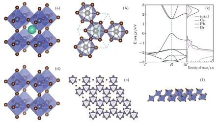
Fig.1. (a)The crystal structure of a cubic ABX3 perovskite,where the green,gray,and brown balls represent the A cations,B cations,and the X anions,respectively;(b)the crystal structure of a cubic perovskite viewed from its[111]direction;(c)the calculated electronic band structure of bulk CsPbBr3, together with its total and site-decomposed DOS; (d) the effective crystal structure of a cubic ABX3 perovskite effectively seen by its low energy charge carriers; (e) the top view of the crystal structure of a BX6 bilayer sliced out along the (111) plane of a cubic perovskite,which constructs the hexagonal honeycomb lattice with two equivalent BX6 sublattices;and(f)the side view of the crystal structure of a hexagonal BX6 bilayer,which indeed presents a buckled single quasi-atom(BX6)layer.
Consequently, a hexagonal perovskite bilayer will naturally present the Dirac-cone electronic states as the graphene at its Dirac points of K and K′. This is a corollary based on the honeycomb symmetry of BX6sublattices and the s- and p-binding characters of BX6octahedra.[1]As a verification example, the hexagonal CsPbBr3bilayer is selected to calculate its electronic band structures near the Fermi level. Here, the DFT calculations are performed within the Perdew-Burke-Ernzerhof (PBE) generalized gradient approximation[27]and the projected augmented wave(PAW) method,[28]as implemented by the Vienna ab initio simulation package (VASP).[29-31]The cutoff energy for the plane-wave basis set is 300 eV and the Brillouin zone is sampled with the Monkhorst-Pack mesh of 6×6×6 for bulk and 6×6×1 for bilayer CsPbBr3. The lattice parameter of bulk CsPbBr3is set to its experimental value a0=5.874 ?A.[32]For the CsPbBr3(111)bilayer,it has the lattice constant of 8.307 ?Aand the thickness of about 6.783 ?A.
As expected,as shown in Fig.2,its top valence and bottom conduction bands disperse linearly and touch each other at K and K′points. Their orbital-decomposed DOS clearly reveals the s- and p-orbital nature of both bands around the Dirac points, and this is further evidenced by the insets of Fig. 2 which plot the isosurfaces of VBM and CBM partial charge densities. By fitting these two bands at k=K+q to the expression vF?E(q)/ˉh|q|,[22]the Fermi velocity is estimated to be vF~0.2×10⁶m/s, which is one fifth of vFof graphene. While graphene has the intrinsic carrier mobility of 2×105cm2·V-1·s-1,[33]it is reasonable to infer that the carrier mobility in such a CsPbBr3bilayer may go around 4×104cm2·V-1·s-1. This makes it rather superior in making ultra-fast electronic devices in comparison with those conventional semiconductors[34]which normally have mobilities less than 104cm2·V-1·s-1.
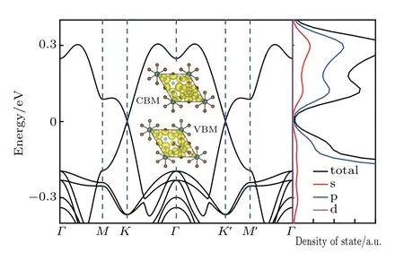
Fig.2.The calculated electronic band structure of a hexagonal CsPbBr3 bilayer(the insets plot the isosurfaces of VBM and CBM partial charge densities),together with its orbital-decomposed DOS.
Moreover, the vacancy-order halide perovskites A3B2X9(A: Cs; B: Fe, Sb, or Bi; X: Cl, Br, or I) are selected to demonstrate the effectiveness of this rule to find the Dirac electronic states away from the Fermi level. Naturally, the A3B2X9perovskites are stacked together by those bilayers of linked BX6octahedra. Figures 3(a)and 3(b)present the crystal structure of Cs3Bi2Br9as an example of the vacancy-order halide perovskites. If viewed from their natural hexagonal axis, the A3B2X9perovskites present the honeycomb lattice of BX6quasi-atoms, as shown in Fig. 3(c). Experimentally,in 1977,the bulk Cs3Bi2Br9crystals were successfully grown by dissolving Bi(OH)3and Cs2CO3in a dilute HBr solution by Lazarini et al.[35]This layered material exhibits trigonal symmetry with a space group of Pˉ3m1 and lattice constants of a=7.972 ?A and c=9.867 ?A.[35]As a stacking unit,its bilayer is inherently stable as graphene to graphite or single-layer h-BN to bulk h-BN. Based on the similar quasi-atom analysis on the CsPbBr3bilayer, the Cs3Bi2Br9bilayer will certainly present the Dirac electronic states as well.
Figure 3(d) shows the calculated electronic band structure of the Cs3Bi2Br9bilayer. And as expected, it presents the crossing Dirac bands as well. However, as Bi contributes one more electron in Cs3Bi2Br9than Pb does in CsPbBr3,its Fermi level goes above the the Dirac bands for the Cs3Bi2Br9bilayer. Its Fermi velocity at the crossing point is found to be vF~0.2×10⁶m/s, which equals the value of the CsPbBr3bilayer. Furthermore, as the layer interaction is rather weak in bulk Cs3Bi2Br9, its electronic band structure exhibits similar Dirac bands below the Fermi level, as shown in Fig.3(e). It is notable that the electronic band structures of A3B2X9perovskites have been previously calculated, such as on Cs3Bi2Br9,[36]or on Cs3Sb2I9.[37]However,in these studies,the Dirac-band features of their band structures were neither noticed nor pointed out.
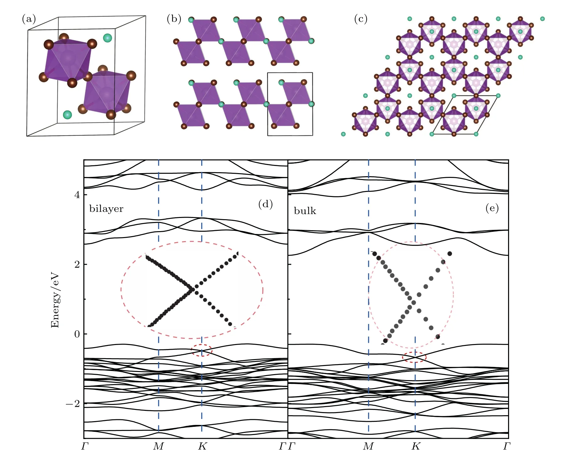
Fig.3. The crystal structures of Cs3Bi2Br9(a)in its primitive cell,(b)from the side view,and(c)from the top view along its natural hexagonal axis,and the calculated electronic band structures of(d)bilayer and(e)bulk Cs3Bi2Br9,where the insets zoom in their Dirac bands below the Fermi level.
In conclusion,we propose a quasi-atom rule for searching 2D Dirac materials in the conventional solids with natural stable bonding lattices. With this rule,we demonstrate with DFT calculations that hexagonal perovskite ABX3bilayers,such as the CsPbBr3(111)bilayer,may have the Dirac band crossing at the Fermi level. Similarly, taking Cs3Bi2Br9as an example,we further demonstrate that the hexagonal vacancy-order halide perovskite A3B2X9bilayers, together with their bulk phases,will have the Dirac bands below the Fermi level. Both CsPbBr3and Cs3Bi2Br9bilayers exhibit the Fermi velocity of ~0.2×10⁶m/s, which makes them promising in making ultra-fast electronic devices.
- Chinese Physics B的其它文章
- Topological magnon insulator with Dzyaloshinskii-Moriya interaction under the irradiation of light?
- Wavelength dependence of intrinsic detection efficiency of NbN superconducting nanowire single-photon detector?
- Artificial solid electrolyte interphase based on polyacrylonitrile for homogenous and dendrite-free deposition of lithium metal?
- Effects of CeO2 and nano-ZrO2 agents on the crystallization behavior and mechanism of CaO-Al2O3-MgO-SiO2-based glass ceramics?
- Modulation of magnetic and electrical properties of bilayer graphene quantum dots using rotational stacking faults?
- Thermal conductivity characterization of ultra-thin silicon film using the ultra-fast transient hot strip method?