基于碳納米薄膜/砷化鎵范德華異質結的高性能自驅動光電探測器研究
2022-03-29 13:04:50霍婷婷張冬冬施祥蕾孫利杰蘇言杰
中國光學 2022年2期
霍婷婷,張冬冬,施祥蕾,潘 宇,孫利杰 ,蘇言杰
(1.上海交通大學 電子信息與電氣工程學院 微納電子學系薄膜與微細技術教育部重點實驗室,上海 200240;2.上海航天技術研究院,上海 201109;3.上海空間電源研究所空間電源技術國家重點實驗室,上海 200245)
1 Introduction
As a typical quasi-one-dimensional nanomaterial, Single-Walled Carbon NanoTubes (SWCNTs)can exhibit semiconduct or metallic according to their diameter and chirality.Moreover, the semiconducting SWCNT has a direct bandgap that is inversely proportional to its diameter[1-2].SWCNT is widely applied to construct high-performance photoelectric devices owing to its ultra-high carrier mobility (105cm2/Vs), high absorption coefficient(104-105/cm) and long exciton diffusion length[3-5].However, strong Coulomb interaction results in the existence of photogenerated electron/hole pairs in the form of excitons after the SWCNT absorbs photons.The exciton binding energy of several hundred meV is directly affected by the SWCNT diameter[6-8].In order to promote effective exciton separation, the application of strong electric fields or the fabrication of heterojunctions is usually pursued to establish strong built-in electric fields.In particular, the strategy of building heterojunctions with other materials, such as bulk semiconductors, nanomaterials and polymers, is widely used to enhance exciton separation and carrier transport[9-16].
With the advantages such as simple structure,simple process and easy interface control, the SWCNT/n-type bulk semiconductor vdW heterojunction, a type of SWCNT-based heterojunction, can fully utilize the ultrahigh carrier mobility of SWCNT and the excellent photoelectric properties of bulk semiconductors[12-18].More importantly, this novel device has broken through the limitation of lattice matching in the growth process of traditional p-n junctions.It can also avoid the disorder interface structure caused by mutual atom diffusion during the formation of vdW heterojunctions, thus facilitating the separation and transport of photogenerated carriers at the interface[19-20].Therefore, the photoelectric devices based on SWCNT/bulk semiconductor vdW heterojunctions are expected to exhibit higher photoelectric response[17-18].In addition,the novel mixed-dimensional vdW heterojunctions with atomic-level interfaces, whose bandgaps are matched with those of bulk semiconductors, can be formed by controlling the diameter/chirality and Fermi level of SWCNTs to facilitate the development of new wide-spectrum photoelectric devices with higher performance.
Different from indirect bandgap semiconductor silicon, gallium arsenide (GaAs) is a direct bandgap semiconductor with better photoelectric performance, more suitable bandgap and higher carrier mobility, and has been widely used in high-efficiency space solar cells.Therefore, the photoelectric devices based on SWCNT/GaAs vdW heterojunctions are expected to exhibit higher photoelectric response than those based on silicon vdW heterojunctions.Liang et al[21].first proved the existence of strong rectification performance in a single SWCNT/n-GaAs heterojunction, and observed obvious photovoltaic effect under irradiation condition.This has laid a foundation for the development of high-performance self-powered SWCNT/GaAs photodetectors.Li et al[22].reported the photovoltaic response of a single SWCNT/n-type GaAs heterojunction.They found that the carrier transport was dominated by thermoelectron emission at low forward bias, while the hole tunneling in the pass interband state mainly contributed to electric current at low reverse bias.Behnam et al[23].studied the Metal-Semiconductor-Metal (MSM) photodetector based on SWCNT film/GaAs Schottky contact, and found that thermoelectron emission was the main transmission mechanism in the SWCNT film/GaAs heterojunction at a temperature above 260 K.The detector exhibited 0.161 A/W photoresponsivity and high switching ratio under 633 nm laser irradiation and 10 V bias.
However, the presence of the SWCNTs with different diameters or mixed conductive properties can easily lead to the non-radiative recombination of carriers in the films, and reduce the separation and transmission efficiency of photogenerated carriers.Therefore, we fabricated a self-powered photodetector based on the p-n vdW heterojunctions by combining (6, 5) enriched SWCNT film with n-type GaAs, and graphene is used to reduce the probability of carrier recombination in SWCNT film and to promote the carrier transport.We tested in detail the wide-spectrum response characteristics of the device in the visible-near infrared band at zero bias.Our results also verify the feasibility of fabricating highefficiency solar cells based on the vdW heterostructures.
2 Experiment
2.1 SWCNT film preparation
SWCNT film has been prepared by vacuum extraction and filtration[24].The specific steps are described as follows.Firstly, 0.5 mg (6, 5)-enriched SWCNT powder (purchased from Sigma-Aldrich)was dispersed into aqueous sodium dodecyl sulfate(SDS) solution (0.01 g/mL) using low-temperature ultrasonic treatment for 2 h.The mixed solution was centrifuged at 14 000 r/min for 20 min to remove the inadequately dispersed SWCNT powder.Then,10 mL centrifuged supernatant was gradually added to the vacuum filtration device with cellulose film(0.22 μm) for filtration and membrane formation.After the mixed solution was filtered, excessive deionized water was added to clean the excess SDS in SWCNT film to reduce its influence on the conductivity of SWCNT film.Finally, the (6, 5)-enriched SWCNT film on cellulose film was dried in a 40°C vacuum oven for 2 h.
2.2 Fabrication of graphene/SWCNT/GaAs vdW heterojunction photodetectors
In this paper, a photoelectric device with vdW heterojunctions was fabricated on a single-side polished n-type GaAs substrate (10 mm×10 mm,20 μm) with AuGeNi eutectic alloy (4 μm) electrode deposited on its back.Firstly, the GaAs substrate was cleaned with acetone, isopropyl alcohol and deionized water successively to remove surface oil stains.Then, an 80 nm Al2O3insulation layer was deposited on the significant surface of GaAs substrate by atomic layer deposition technology, and a 3 mm×3 mm window was opened in its middle.Subsequently, the GaAs substrate was immersed in(NH4)2S solution for 30 min to passivate the GaAs surface within the window, and excess (NH4)2S solution was removed with deionized water.Later,the prepared SWCNT film (7 mm×7 mm) was transferred above the patterned window and directly contacted with GaAs to form the SWCNT/GaAs vdW heterojunctions, and the cellulose film was dissolved and removed by slowly dripping acetone.The graphene was then transferred to the upper surface of SWCNT film by wet process.Finally, the graphene /SWCNT/GaAs vdW heterojunction photodetector was obtained by applying silver paste on the graphene surface around the window to form ohmic contact.
2.3 Testing and characterization
The surface morphologies of the graphene/SWCNT film/GaAs vdW heterojunction were characterized by Scanning Electron Microscopy (SEM)(Zeiss Ultra Plus, Germany).The Raman peak shift of the heterojunction was performed Via Renishaw Raman spectroscopy with an excitation wavelength of 514 nm.The photoelectric performance of the device was evaluated using Agilent 4156C semiconductor parameter analyzer at room temperature, and the current-voltage (I-V) curve and current-time (IT) curve were measured by irradiation with 405-1 064 nm laser and AM1.5G standard solar simulator.The frequency response curve of the device was measured by a chopper (4-400 Hz) and a digital oscilloscope (Tektronix, TDS 3052C).

Fig.1 (a) Schematic diagram of graphene/SWCNT film/GaAs vdW heterojunction photodetector structure; (b) SEM image of graphene/SWCNT film圖1 (a)石墨烯/SWCNT膜/GaAs vdW異質結光電探測器結構示意圖;(b)石墨烯/SWCNT薄膜的SEM圖片
3 Result and discussion
The structure of the fabricated graphene/SWCNT film/GaAs vdW heterojunction photodetector is shown in Figure 1(a).It can be clearly seen that this is a p-n heterojunction structure directly formed by(6, 5)-enriched SWCNT film and n-type GaAs, significantly different from the previous SWCNT network/graphene/GaAs heterojunction photodetector,which is a Schottky heterojunction[25].In this paper,the use of (6, 5)-enriched SWCNT film can improve the absorption of photons in bands smaller than GaAs bandgap.On the other hand, the Fermi level of SWCNT film can be later regulated by doping to better facilitate the fabrication of high-performance wide-spectrum photodetectors.Here, graphene mainly plays a role in promoting the transport of photogenerated carriers in the SWCNT film.Figure 1(b) shows a typical SEM image of graphene/SWCNT film/GaAs vdW heterojunction surface in the window area.It can be clearly seen that SWCNT and graphene forms a uniform meshed film on the GaAs surface, and no obvious residue of surfactant SDS is observed, indicating that the SDS removal is relatively thorough in the process of SWCNT film filtration.This will help improve the photoelectric performance of vdW heterojunction devices.
We first tested theJ-Vcurve of the graphene/SWCNT film/GaAs vdW heterojunction photodetector in dark state and AM1.5G light condition, as shown in Figure 2.It can be clearly seen from theJVcurve for dark state that the device has an obvious rectification effect, indicating that the (6, 5)-enriched SWCNT film is combined with GaAs into a good p-n junction in the device.It should be noted that the current density of device in the first quadrant is low.Under the AM1.5G standard solar radiation, theJ-Vcurve obviously moves downward,and the short-circuit current density (Jsc) of device rises up to 19 mA/cm2, an indicator of excellent photovoltaic performance.This indicates that the device has the potential to build efficient solar cells.The rectification performance of the device is analyzed based on the classical thermoelectron emission principle:

Fig.2 Typical J-V curves of graphene/SWCNT film/GaAs vdW heterojunction photodetector in (a) dark state and (b) AM 1.5G condition圖2 石墨烯/SWCNT膜/GaAs vdW異質結光電探測器在(a)暗態和(b)AM 1.5G條件下的J-V曲線
whereJstis the reverse saturation current density,Tis the absolute temperature,k0is Boltzmann constant,A* is the effective Richardson constant, andΦnsis the barrier height.From theJ-Vcurve for dark state, it can be concluded that the saturation current density (Jst) is 9.93×10⁻⁷A/cm2, and that the thermoelectron emission plays a dominant role in carrier diffusion and generation recombination.However,the increase of current density drops sharply in the first quadrant, which may be related to the existence of the reverse junction.As a result, theJ-Vcurve of the device is different from the existing result, but the open-circuit voltage is not significantly affected and is still 0.63 V.Therefore, the graphene/SWCNT film/GaAs vdW heterojunction is mainly viewed as a self-powered photoelectric device and is evaluated in terms of detection performance.
In order to evaluate the detection performance of the graphene/SWCNT film/GaAs vdW heterojunction devices as self-powered photodetectors, we measured the photoelectric response at different laser wavelengths at room temperature, as shown in Figure 3 (Color online).Figure 3(a)~(b) shows the typicalJ-Vcurves of the graphene/SWCNT film/GaAs vdW heterojunction photodetectors under laser irradiation at different wavelengths.It can be clearly seen that allJ-Vcurves move downward at different laser wavelengths, indicating that the vdW heterojunction devices exhibit obvious photovoltaic effect.In particular, the maximum short-circuit current density (Jsc) of the device can reach 22.48 mA/cm2under the irradiation of 405 nm laser with 30 mW/cm2optical power density.It is worth noting that the device can still produce a relatively obvious photovoltaic effect under 1 064 nm laser irradiation.The downward shift ofJ-Vcurve to break through the 860 nm absorption limit of GaAs is mainly caused by the existence of (6, 5)-enriched SWCNT film in the heterojunction.Thus, the photoinduced carriers generated by (6, 5)-enriched SWCNT film after absorbing photons can be separated into electron-hole pairs at the heterojunction interface and exported to the external circuit to form a photocurrent dominating the photoelectric response process of the device.The introduction of graphene can help enhance the transport of holes in the SWCNT film and improve the ability of charge collection.Therefore, the subsequent optimization of graphene, the thickness and Fermi level of SWCNT film, bandgap and the SWCNT-GaAs interface contact will be expected to further improve the photoelectric response characteristics in long-wave band.Figure 3(c)~(d) shows the stability curves of the graphene/SWCNT film /GaAs vdW heterojunction photodetector irradiated at different laser wavelengths.It can be clearly seen that the photocurrent density increases or decreases rapidly with the laser on or off, and the device exhibits fast photoelectric response and excellent photoelectric response stability under 405-1 064 nm laser illumination.Moreover, the device shows a high switching ratio, which is greater than 1.1×10³under 406~860 nm laser illumination and is 2.5 even when irradiated by 1 064 nm laser.

Fig.3 (a) (b) J-V curves of the graphene/SWCNT film/GaAs vdW heterojunction photodetector irradiated at different laser wavelengthes.(c) (d) Photoelectric response repeatability curves when irradiated by laser with different laser wavelengthes at zero bias圖3 (a)和(b) 不同激光波長輻照下石墨烯/SWCNT膜/GaAs vdW異質結光電探測器的J-V曲線;(c)和(d) 零偏壓時不同激光波長輻照下的光電響應重復性曲線
In addition, we tested the transient light re- sponse of the device at 200 Hz frequency and 405 nm laser wavelength, as shown in Figure 4.It can be seen that the photodetector shows a fast response speed when switching the on/off state.The photoelectric response curve is still complete at the frequency of 200 Hz.When the frequency is further increased, the photoelectric response of the photodetector begins to decline before reaching a maximum.Thus, the maximum response frequency of the selfpowered photoelectric device based on graphene/SWCNT film/GaAs vdW heterojunction is 200 Hz.In addition, the photoelectric response time of the device can be extracted from the photoelectric response curve.In general, the response (tr)/recovery(tf) time of the device is defined as the time required for the photoelectric current to rise/fall to 90%/10% of the maximum photocurrent, respectively.From Figure 4, the response (tr)/recovery (tf)time can be determined as 60 μs and 910 μs, respectively.The response time of tens of microseconds indicates the ultra-fast carrier separation efficiency at the SWCNT/GaAs interface and the ultra-high charge transport efficiency of the whole graphene/SWCNT film/GaAs vdW heterojunction photodetector.
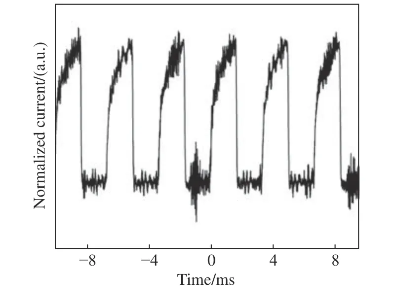
Fig.4 Transient light response curve of the device under 405 nm laser irradiation圖4 405 nm激光輻照條件下器件的瞬態光響應曲線
We further evaluated the photoelectric responsivity (R) and specific detectivity (D*) of the graphene/SWCNT film/GaAs vdW heterojunction photodetector.TheRandD* values at different laser wavelengthes can be obtained according to the following formula:

whereIpis the photocurrent,Idis the dark current,Pinis the incident light power, andAis the effective area (9 mm2).By changing the laser wavelength and incident power density, the change values ofRandD* values of the graphene/SWCNT film/GaAs vdW heterojunction photodetector are obtained, as shown in Figure 5.It can be seen from the photoelectric response curves in Figure 5(a)-(b) that the photoelectric responsivity of the device increases as a whole with decreasing the incident power density.This change trend basically accords with the general law of photo detector, this is because the incident light can be absorbed by the device and be fully converted into current with the decrease of the incident power.From Figure 5(a), the maximumRvalue of the self-powered photodetector under 405 nm laser irradiation can reach 1 214 mW/cm2, which is higher than the values reported in previous studies[24].Although the photoelectric response of the device at 980-1 064 nm is 3 orders of magnitude lower than that at 405-860 nm, this result still demonstrates the feasibility that the graphene/SWCNT film/GaAs vdW heterojunctions fabricated in this paper can further broaden the spectral response range.Subsequently, high photoelectric responsivity can be expected at 405-1 064 nm by optimizing the relative thickness of SWCNT and GaAs until their light absorption is of the same order of magnitude.Figure 5(c)~(d) shows the specific detectivity curves of the device under different laser wavelengths and optical power densities.Similar to the photoelectric responsivity, the specific detectivity also increases as a whole with decreasing incident power density,and the maximum specific detectivity of 2×10¹²Jones can be obtained at 405 nm laser wavelength with the power density of 5 mW/cm2.
In order to better understand the working mechanism of the graphene/SWCNT film/GaAs vdW heterojunction photodetector, we analyze the energy band structure and charge transfer process at the interface.Since the SWCNTs used in this paper is a (6, 5)-enriched semiconducting SWCNTs, the energy band structure of (6, 5) SWCNTs is used to analyze the energy band structure of SWCNT/GaAs heterojunction and its working mechanism is discussed.As we know, the Dirac point of graphene is 4.6 eV, and (6, 5) SWCNT exhibits a weak p-type with a conduction band of 3.9 eV and a valence band of 5.1 eV.The Fermi level of n-type GaAs is close to its 4.07 eV conduction band, and the energy band structure of the vdW heterojunction is shown in Figure 6.When (6, 5) SWCNT contacts with n-type GaAs, a II-type heterojunction can be formed due to the difference between their conduction bands and valence bands.According to the band theory, the static electron transfer from n-type GaAs to (6, 5) SWCNT happens after the contact,which can be confirmed by Raman spectrum[24].A built-in electric field is formed between graphene/(6,5) SWCNT and n-type GaAs, resulting in the bending of their energy bands.When the excitation wavelength is shorter than 860 nm, the electron/hole pairs are generated in (6, 5) both SWCNT and ntype GaAs, and then will be separated and transported to the external circuit under the action of the built-in electric field at the interface.The photogenerated holes in n-type GaAs drift towards the (6, 5)SWCNT side, and then are collected by electrodes and transported to the external circuit.However,when the excitation wavelength of laser exceeds the absorption limit of n-type GaAs, the optical absorption of the device mainly comes from (6, 5) SWCNT film, the photo-induced electron-hole pairs are separated by the built-in electric field at the SWCNT/GaAs heterojunction interface, and the photoinduced electrons are transferred to the external circuit through n-type GaAs.The existence of graphene is conducive to reduce the probability of photo-generated carrier combination during the transport in SWCNT film so that more holes will be transport to the external circuit.Therefore, when the excitation wavelength is larger than 860 nm, the graphene/(6, 5) SWCNT film dominates the photoelectric response process.
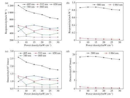
Fig.5 The responsivity (a~b) and specific detectivity (c~d) of graphene/SWCNT film/GaAs vdW heterojunction photodetectors as a function of incident light power density under zero bias conditions圖5 零偏壓條件下石墨烯/SWCNT膜/GaAs vdW異質結光電探測器的(a~b)光電響應度和(c~d)比探測率隨入射光功率密度改變而變化的曲線
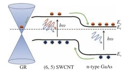
Fig.6 Schematic diagram of the energy band structure of graphene/SWCNT film/GaAs vdW heterojunction exposed to light irradiaton圖6 石墨烯/SWCNT膜/GaAs vdW異質結在光照時的能帶結構示意圖
4 Conclusion
In conclusion, we report a self-powered photodetector based on graphene/SWCNT film/GaAs vdW heterojunction, in which, the p-n junction formed by (6,5)-enriched SWCNT film and n-type GaAs plays a dominate role, while graphene is used to reduce the probability of carrier recombination in SWCNT film and promote the carrier transport.The experimental results show that the self-powered photodetector based on graphene/SWCNT film/GaAs vdW heterojunction exhibits a sensitive photoelectric response to 405-1 064 nm visible-near infrared light, breaking through the absorption limit of GaAs, and demonstrating the feasibility of further broadening the spectral response range of a GaAsbased photodetector based on vdW heterojunction.The photoelectric responsivity and specific detectivity of the device under 405 nm laser irradiation can reach 1.214 A/W and 2×10¹²Jones respectively.It may be attributed mainly to the light absorption of n-type GaAs and the formation of vdW heterojunction.By further optimizing the structure and parameters, the devices based on graphene/SWCNT film/GaAs vdW heterojunctions are expected to be used as high-efficiency solar cells and wide-spectrum photodetectors.
——中文對照版——
1 引 言
作為典型的準一維納米材料,單壁碳納米管(SWCNT)根據其直徑和手性表現出半導體型和金屬型,而且半導體型SWCNT為直接帶隙且其帶隙與直徑成反比例關系[1-2],超高的載流子遷移率(105cm2/ Vs)、高吸收系數(104-105/cm)和長激子擴散長度使得SWCNT被廣泛應用于構筑高性能光電器件[3-5]。但是,較強的庫侖相互作用導致SWCNT吸收光子后所形成的光生電子/空穴對以激子的形式存在,其數百meV的激子結合能受SWCNT直徑直接影響[6-8]。為了促進激子的有效分離,通常采用施加強電場或構建異質結的方式以便形成較強的內建電場。尤其是,通過與其他材料(例如體半導體、納米材料和聚合物)構建異質結的策略被廣泛用于增強激子分離和載流子輸運[9-16]。
在SWCNT基異質結中,SWCNT /n型體半導體范德華(van der Waals, vdW)異質結可以同時利用SWCNT的超高載流子遷移率以及體半導體的優異光電性能,具有結構簡單、工藝簡便、易于調控界面等優點[12-18]。更重要的是,這種新型器件結構突破了傳統pn結在生長工藝中所受晶格匹配的限制,而且還可以避免vdW異質結形成過程中原子相互擴散導致的界面無序結構,進而有利于光生載流子在界面處的分離和輸運[19-20]。因此,基于SWCNT /體半導體vdW異質結的光電器件有望表現出更高的光電響應特性[17-18]。另外,通過調控SWCNT的直徑/手性、費米能級等參數可以與體半導體形成能帶匹配、具有原子級界面的新型混合維度vdW異質結,有利于開發更高性能的新型寬光譜光電器件。
與間接帶隙半導體硅不同,砷化鎵(GaAs)是一種具有更優異光電性能的直接帶隙光電半導體,其具有更合適的帶隙和更高的載流子遷移率,并已經被廣泛用于高效空間太陽能電池。因此,基于SWCNT/GaAs vdW異質結的光電器件有望比硅基vdW異質結光電器件表現出更高的光電響應特性。Liang等[21]首先證明了在單根SWCNT/n-GaAs異質結中有很強的整流性能,并且在光照下觀察到了明顯的光伏效應,這為高性能自供電SWCNT/GaAs光電探測器奠定了基礎。Li等[22]報道了單根SWCNT/n型GaAs異質結的光伏響應。發現載流子傳輸在低正向偏壓下由電子熱電子發射占主導,而通過帶間狀態的空穴隧穿主要在低反向偏壓下貢獻電流。Behnam等[23]研究了基于SWCNT薄膜/GaAs肖特基接觸的金屬-半導體-金屬(MSM)光電探測器,并發現在260 K以上的溫度條件下,熱電子發射是SWCNT膜/ GaAs異質結中的主要傳輸機制。該探測器在633 nm激光輻照和10 V偏壓條件下表現出0.161 A/W的光電響應度和高開關比。
但是,不同直徑或混合導電屬性碳納米管的存在導致SWCNT薄膜中的載流子極易發生非輻射復合,從而降低了光生載流子的分離和傳輸效率。因此,本論文采用以(6,5)手性為主的SWCNT薄膜與n型GaAs構建p-n結,并利用石墨烯降低SWCNT薄膜內載流子的復合幾率和促進載流子傳輸,構筑了基于這種新型 vdW異質結的自驅動光電探測器,詳細研究了該器件在零偏壓條件對可見-近紅外波段的寬光譜響應特性。本文研究驗證了基于該vdW異質結構筑高效太陽能電池的可行性。
2 實驗部分
2.1 SWCNT薄膜制備
SWCNT薄膜采用真空抽濾的方法制備[24],具體步驟如下:首先將0.5 mg (6,5)手性為主的SWCNT粉體(購自Sigma-Aldrich)分散到十二烷基硫酸鈉(SDS)水溶液(0.01 g/mL)中低溫超聲處理2 h,并將混合溶液以14 000 r/min的速度離心20 min,去除未充分分散的SWCNT。然后,取10 mL離心后的上清液逐步滴加到放置有纖維素膜(0.22 μm)的真空抽濾裝置中進行抽濾成膜,待混合溶液濾過后添加過量的去離子水清洗SWCNT膜中多余的SDS,以降低其對SWCNT薄膜導電性的影響。最后,將纖維素膜上(6,5)手性為主的SWCNT薄膜放入40 °C真空烘箱中干燥2 h備用。
2.2 石墨烯/SWCNT/砷化鎵vdW異質結光電器件構筑
本論文選用背面已沉積AuGeNi共晶合金(4 μm)電極的單面拋光n型GaAs襯底(10 mm×10 mm,20 μm)構筑vdW異質結光電器件。首先將GaAs襯底依次用丙酮、異丙醇和去離子水清洗去除表面油污。然后利用原子層沉積技術在GaAs襯底正表面上沉積一層厚度為80 nm的Al2O3絕緣層,并且中間開有3 mm×3 mm的窗口。隨后,將GaAs襯底浸入(NH4)2S溶液中,放置30 min,以鈍化窗口內的GaAs表面,并用去離子水清洗去除多余的(NH4)2S溶液。最后,將上述制備的SWCNT薄膜(7 mm×7 mm)轉移到圖案化窗口上方,直接與GaAs直接接觸形成SWCNT /砷化鎵vdW異質結,并緩慢滴加丙酮浸泡溶解去除纖維素膜。隨后將石墨烯通過濕法轉移方式轉移到SWCNT薄膜上表面。最后,在窗口周圍的石墨烯表面涂覆銀漿以形成歐姆接觸,獲得石墨烯/SWCNT/GaAs vdW異質結光電探測器。
2.3 測試與表征
本文使用掃描電子顯微鏡(SEM,Zeiss Ultra Plus, Germany)表征石墨烯/ SWCNT膜/砷化鎵范德華異質結表面的微觀形貌;使用inVia Renishaw拉曼光譜儀測試異質結的Raman峰偏移,其中激發波長是514 nm;器件的光電性能則使用安捷倫4156C半導體參數分析儀在室溫條件下進行測量,在405~1 064 nm激光和AM1.5G標準太陽光模擬器輻照下測得電流電壓(I-V)曲線和電流時間(I-T)曲線。器件的頻率響應曲線則采用斬波器(4~400 Hz)和數字示波器(Tektronix,TDS 3052C)進行測試。
3 結果與討論
所構筑的石墨烯/SWCNT薄膜/GaAs vdW異質結光電器件的結構示意圖如圖1(a)所示。可以清楚看出,在該異質結結構中(6,5)手性為主的SWCNT薄膜直接與n型GaAs形成p-n結,這與之前的SWCNT網絡/石墨烯/GaAs異質結光電器件有顯著區別,后者所形成的是肖特基異質結[25]。采用(6,5)手性為主的SWCNT薄膜一方面有利于提高器件對小于GaAs帶隙的波段光子的吸收,另一方面,后續可通過摻雜來調控SWCNT薄膜費米能級從而更有利于制備高性能的寬光譜光電探測器。本文中,石墨烯主要起到促進光生載流子在SWCNT薄膜傳輸的作用。圖1(b)為窗口區域內石墨烯/SWCNT膜/GaAs vdW異質結表面的SEM圖片,可以清楚地看到,GaAs表面SWCNT與石墨烯一起形成均勻的網狀薄膜,并且沒有觀察到明顯的表面活性劑SDS殘余,說明SWCNT薄膜抽濾過程中SDS去除較為干凈,這將有助于提高vdW異質結器件的光電性能。
首先測試了石墨烯/SWCNT膜/GaAs vdW異質結光電探測器在暗態和AM1.5G光照條件下的J-V曲線,結果如圖2所示。從暗態J-V曲線可以清楚地看出,器件具有明顯的整流效應,表明該器件中(6,5)手性為主的SWCNT薄膜與GaAs形成了較好的p-n結,需要說明的是器件在第一象限時的電流密度較低。當采用AM1.5G標準太陽光輻照時,J-V曲線發生明顯向下移動,器件的短路電流密度Jsc可達19 mA/cm2,顯示出優異的光伏特性,由此說明,器件具有構筑高效太陽電池的潛力。基于經典的熱電子發射原理來分析器件的整流性能:
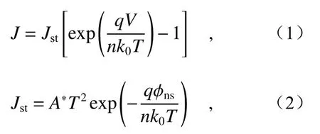
其中,Jst是反向飽和電流密度,T是絕對溫度,k0是玻爾茲曼常數,A*是有效理查森常數,?ns是勢壘高度。從暗態的J-V曲線可以得出飽和電流密度Jst為9.93×10⁻⁷A/cm2,并且熱電子發射在載流子擴散和生成復合機制中起主導作用。但是需要指出的是,在第一象限時器件的電流密度增加急劇下降,這可能與反向結的存在有關系,最終導致該器件的J-V曲線不同于已有結果,但開路電壓并未受到較大影響,仍有0.63 V。因此,對于本文所構筑的石墨烯/SWCNT膜/GaAs vdW異質結,主要用作自驅動光電器件,并詳細評價其探測性能。
為了評估石墨烯/SWCNT膜/GaAs vdW異質結器件作為自驅動光電探測器的探測性能,測量了室溫條件下不同激光波長輻照下的光電響應曲線,結果如圖3所示(彩圖見期刊電子版)。圖3(a)和圖3(b)展示了不同波長激光輻照條件下的石墨烯/SWCNT膜/ GaAs vdW異質結光電探測器的典型J-V曲線。可以清楚地看出,所有J-V曲線在不同波長激光輻照下均向下移動,表明該vdW異質結器件均可產生明顯的光伏效應。尤其是,在光功率密度為30 mW/cm2的405 nm激光輻照條件下,器件的最大短路電流密度Jsc可達到22.48 mA/cm2。值得注意的是,該器件在1 064 nm激光輻照下仍然能夠產生較為明顯的光伏效應,J-V曲線下移,突破了砷化鎵860 nm的吸收極限,這主要是由異質結中(6,5)手性為主的SWCNT薄膜引起的。由此說明,(6,5)手性為主的SWCNT薄膜吸收光子后產生的光生載流子可以在異質結界面處被分離成電子-空穴對,并被導出到外電路形成光電流,主導了器件的光電響應過程。而石墨烯的引入則有利于增強SWCNT薄膜內空穴的傳輸,提高電荷收集能力。因此,后續通過優化石墨烯和SWCNT薄膜厚度和費米能級、SWCNT帶隙及其與GaAs之間的界面接觸,將有望進一步提高長波波段的光電響應特性。圖3(c)和圖3(d)展示了在不同激光波長輻照條件下石墨烯/SWCNT膜/GaAs vdW異質結光電器件的穩定性曲線。可以清楚地看出,光電流密度隨著激光打開或關閉迅速增加或降低,器件對405~1 064 nm波段的激光表現出快速的光電響應和優異的光電響應穩定性。而且器件具有較高的開關比,對406~860 nm激光輻照時開關比均大于1.1×10³,即便采用1 064 nm激光輻照時器件的開關比仍有2.5。
此外,還測試了器件在200 Hz頻率和405 nm激光輻照條件下的瞬態光響應曲線,如圖4所示。可以看出,光電探測器在開/關狀態切換時表現出較快的響應速度;當頻率為200 Hz時,光電響應曲線仍然是完整的,當進一步增大頻率時,光電探測器的光電響應未達到最大值便開始下降。由此說明,石墨烯/SWCNT膜/GaAs vdW異質結自驅動光電器件的最大響應頻率是200 Hz。另外,根據這個光電響應曲線,可以提取器件的光電響應時間。通常情況下,器件的響應(tr)/恢復(tf)時間分別被定義為光電電流上升/下降到最大光電流90%/10%時所需的時間,從圖4曲線可知,該器件的(tr)/(tf)分別為60 μs和910 μs。數十μs級的光電響應時間再次表明SWCNT/GaAs異質結界面處的超快載流子分離效率以及整個石墨烯/SWCNT膜/GaAs vdW 異質結光電器件的超高電荷輸運效率。
進一步評估了石墨烯/SWCNT膜/GaAs vdW異質結光電器件的光電響應度(R)和比探測率(D),其在不同激光波長輻照條件下的光電響應度和比探測率數值為:

其中,Ip是光電流,Id是暗電流,Pin是入射光功率,A是有效面積(9 mm2)。通過改變激光波長和入射功率密度,石墨烯/SWCNT膜/GaAs vdW異質結光電器件的光電響應度和比探測率曲線分別如圖5(彩圖見期刊電子版)所示。從圖5(a)~5(b)中的光電響應度曲線可以看到,器件的光電響應度隨著入射功率密度的增加而降低,這一變化趨勢基本符合光電探測器的一般規律,其原因在于隨著入射光功率密度的降低,入射光可以被器件吸收并被充分轉換成光電流。由圖5(a)可以得到該自驅動光電探測器在405 nm激光輻照條件下的光電響應度最大可達1 214 mW/cm2,高于已有研究報道的數值[24]。盡管器件在980~1 064 nm波段的光電響應度比405~860 nm波段低了3個數量級,但這一結果仍然說明了本文所構筑的石墨烯/SWCNT膜/GaAs vdW異質結具有進一步拓寬光譜響應范圍的可行性,后續通過優化SWCNT與GaAs的相對厚度可使兩者的光吸收具有相同的數量級,將有望在405~1 064 nm波段實現較高的光電響應度。圖5(c)~5(d)為器件在不同激光波長和光功率密度條件下的比探測率曲線。可以清楚地看出,比探測率與光電響應度相似,也隨著入射光功率密度的降低而整體上增加,并且在405 nm激光以5 mW/cm2的功率密度輻照下獲得了最大比探測率,為2×1012Jones。
為了更好地理解石墨烯/SWCNT膜/GaAs vdW異質結光電探測器件的工作機理,從能帶結構和界面電荷轉移的角度進行分析。由于本文中所采用的SWCNT是以(6,5)手性為主的純半導體性SWCNT,因此分析SWCNT/GaAs異質結的能帶結構時采用(6,5)SWCNT的能帶結構來討論該器件的工作機理。石墨烯的狄拉克點為4.6 eV,而(6, 5) SWCNT表現出弱p型,其導帶為3.9 eV,價帶為5.1 eV。n型GaAs費米能級接近其4.07 eV的導帶,因此,該vdW異質結的能帶結構示意圖如圖6所示。當(6, 5) SWCNT和n型GaAs接觸時,由于兩者的導帶和價帶差異而形成Ⅱ型異質結。根據能帶理論,接觸后會發生從n型砷化鎵到 (6, 5) SWCNT靜態電子轉移,這可以通過拉曼光譜獲得證實[24]。在石墨烯/(6, 5) SWCNT和n型砷化鎵之間產生了內建電場,并使(6, 5) SWCNT和n型GaAs的能帶彎曲,當激發波長小于860 nm時,(6, 5) SWCNT和n型GaAs中均會生成電子/空穴對,然后在界面處內建電場的作用下分離傳輸到外電路,n型GaAs中的光生空穴向(6, 5) SWCNT側漂移,然后被電極收集并傳輸到外電路。但是,當激光的激發波長超過n型GaAs的吸收極限時,器件的光吸收主要源自(6, 5) SWCNT薄膜,所產生的光生電子空穴對在SWCNT/GaAs異質結界面處由于內建電場的作用而發生分離,光生電子通過n型GaAs被傳輸到外電路。石墨烯的存在有利于降低光生空穴在SWCNT薄膜傳輸過程中的復合幾率。使得更多的光生空穴傳輸到外電路。因此,當激發波長大于860 nm時,石墨烯/(6, 5) SWCNT薄膜主導光電響應過程。
4 結 論
本文報道了一種基于石墨烯/SWCNT膜/GaAs vdW異質結的自驅動光電探測器件,其中由(6,5)手性為主的SWCNT薄膜與n型GaAs所形成的p-n結起主導作用,石墨烯起到降低SWCNT薄膜內載流子復合幾率和促進載流子傳輸作用。實驗結果表明,基于石墨烯/SWCNT膜/GaAs vdW異質結的自驅動光電探測器對405~1 064 nm波段的可見-近紅外光具有較為靈敏的光電響應,突破了GaAs的吸收極限,驗證了基于該vdW異質結進一步拓寬GaAs基光電器件光譜響應范圍的可行性。器件在405 nm激光輻照下的光電響應度和比探測率分別可達1.214 A/W和2×1012Jones,這主要歸因于n型砷化鎵的光吸收和vdW異質結的形成。通過進一步優化器件結構和參數,基于石墨烯/SWCNT膜/GaAs vdW異質結的器件有望被用于構筑高效太陽電池和寬光譜光電探測器。