基于0.13μm CMOS 工藝的全集成北斗導航射頻接收機*
2012-08-09 08:08:32曾隆月黃繼偉張常紅王永平
電子器件 2012年6期
曾隆月,黃繼偉 ,張常紅,王永平
(1.廣州潤芯信息技術有限公司,廣州 510663;2.東南大學射光所,南京 210096)
The Global Positioning System(GPS)has many applications,such as emergency search,military usage,time report and positioning;therefore,the market of this positioning system is perspective.With the developing of this market,more attention has been paid to the design and implementation of GPS radio receiver to achieve low power,low cost and small size[1-5].Russian,European and China,after the USA,are supposed to be developing their own Positioning System.However,less research has been made to design state-of-the-art radio receiver for those systems.In this paper,we focus on the implementation of the radio receiver for Compass Navigation Satellites System(CNSS,also known as Beidou).
The Chinese government has set up the CNSS plan in 2000.At the end of 2010 nine satellites have been launched,and another 26 satellites would be launched in the next ten years after the entire navigation system has been completed.The signal of CNSS for global civil usage is called B1 band,and its frequency is 1 561.098 MHz with bandwidth 4.092 MHz.The minimum B1 signal strength received at the antenna port is about-130 dBm,which is 22 dB below the thermal noise.By despreading and integrating over a long time period,a receiver can exploit the inherent spread-spectrum processing gain of the navigation signals to get the proper postcorrelation signal-to-noise ratio(SNR).
In this paper,the design and implementation of a state-of-the-art CNSS radio receiver is firstly presented.This low-IF receiver is fully integrated,including power regulator,local oscillator and 2 bits analog to digital converter(ADC).The system requirements and architecture of the CNSS radio receiver are presented in Section Ⅱ.Section Ⅲdescribes the circuit implementation of the CNSS receiver,and Ⅳ describes the measured performance and its analysis.Conclusion is made in Sections Ⅴ.
1 Receiver Requirements and Architecture
To satisfy the stringent power and area requirements,it is necessary to properly specify and optimize the receiver requirement;however,there is no radio transmission standard for the CNSS system.Fortunately,since CNSS signal is almost the same as the GPS,except that its frequency and bandwidth is different as mentioned above,we can deduce the requirement for CNSS receiver from the Reference [4],which well defines the specification of GPS.According to the reference,the specification of CNSS radio receiver is shown as Table 1.There are almost no linearity requirements for both CNSS and GPS receiver,since the input signals at the antenna port are very weak.The input compresses point(ICP)of-80 dBm is enough.However,in our work,there are no external filters used to achieve lower noise;so the strong signal from GSM and DCS can be seen as the interferers.The ICP requirement is-23 dBm and-25 dBm at those frequencies,respectively.
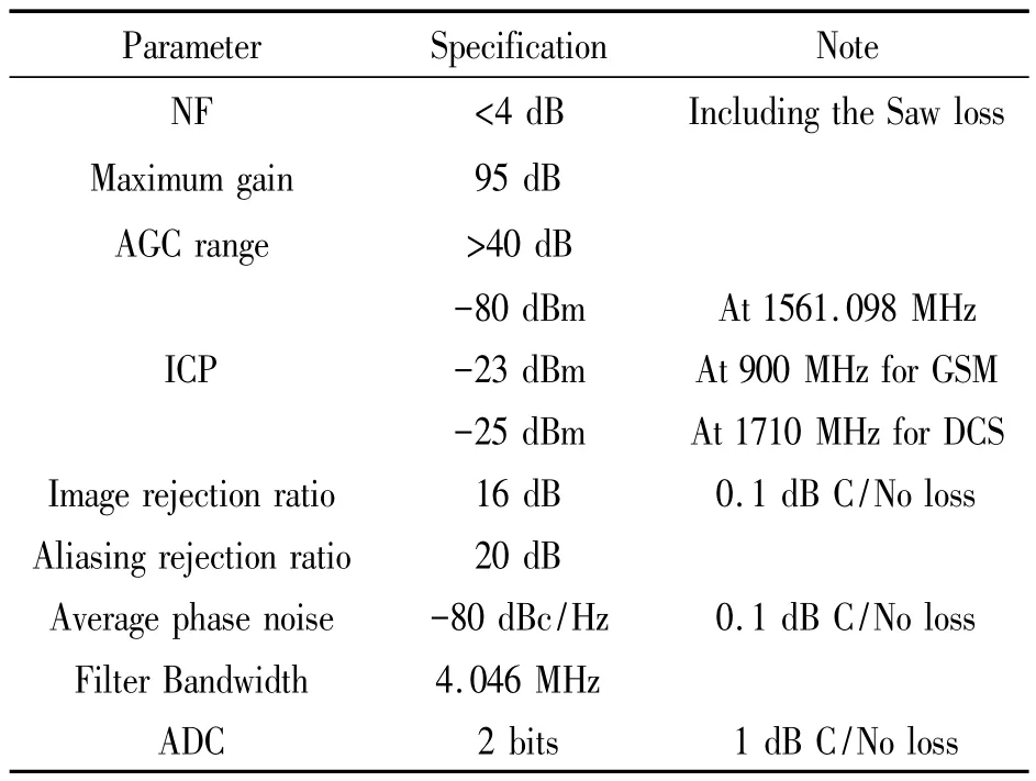
Table 1 the radio specification for CNSS
In CNSS B1 band,even wider bandwidth than necessary for the C/A code was reserved for P code,and there are no blocking signals nearby.The only image signal is the thermal noise,so the image rejection ratio requirement is simple.In order to keep the C/No(Carrie to noise density)less than 0.1 dB,the image rejection ratio of 16dB is sufficient[4].Due to this simple image rejection ratio and highly integration requirement,the low-IF or zero-IF instead of superheterodyne architecture receiver should be selected.Given CMOS implementation(i.e.,presence of flicker noise)and the nature of the CNSS signal(where a significant amount of energy is contained at the center of frequency),a zero-IF implementation is impractical.For this reason,a low-IF architecture has been preferred for the front-end section as shown in Fig.1.In this receiver,the complete analog building blocks are integrated,including a low noise amplifier(LNA),a Quadrature mixer,auto gain control amplifier and channel-select filter,a 2-bit ADC,power regulator and a phase-locked loop(PLL).All the circuitry is differential to reduce substrate noise injection,coupling and the LO interfering,which is an important consideration because of the high total voltage gain(≈95 dB).In this receiver,the poly-phase filter is used to eliminate the image signal.The IF is about 4.175 MHz as it represents a good trade-off between gain×bandwidth in IF section and low 1/f noise in the I &Q Mixer.
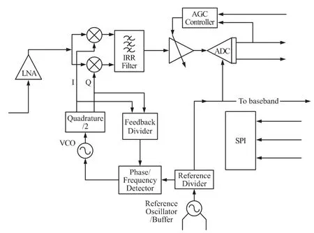
Fig.1 The architecture of the CNSS receiver
2 Circuit Implementation
2.1 RF Section
The cascaded,inductive source-degenerated lownoise amplifier (LNA)depicted in Fig.2 is a fully balanced architecture as it is immune to the noise from power regulator and substrate.This LNA is co-designed with the ESD since it typically worsens LNA performance.
As in Fig.2 the cascode configuration LNA is adopted to improve the reverse isolation and reduce the Miller capacitance between the Mxa-Mxb.A 7.2-nH differential on-chip inductor with a quality factor Q >12 resonates with the load CLand the parasitic capacitor at the input of Mixer.The load capacitor CLis a digitally controlled capacitor bank that can be tuned to compensate for process and temperature variations.At resonate frequency,the impedance of the tuned LC tank is primarily determined by the quality factor(Q)of the inductors.Thus the inductors L1and their physical dimensions are optimized to give the highest Q,which translates to a high voltage gain.The LNA is required to provide sufficiently high voltage gain in order to satisfy the front-end's noise requirements.In the LNA design,there is usually a trade-off between high gain,low noise and linearity.However in the CNSS LNA design,we focus on almost only the high gain and low noise due to its simple linearity requirements.
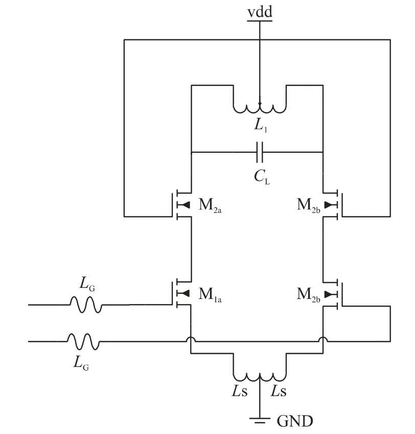
Fig.2 The simplified schematic of LNA
For area saving and noise reducing considerations,a bond wire is used as the source-degenerated inductor Lsfor its high quality factor.The 50Ω input match is achieved with the combination of the bond wire Lsand the off-chip inductor Lg.The input impedance seen at the input of the LNA is
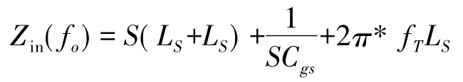
where fTis the cut-off frequency of M1,Cgsis the gatesource capacitance of MOS M1,and fois the resonate frequency,where the imaginary part is concealed,and the input impedance is given by:
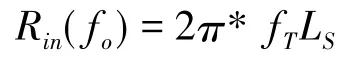
The input match is achieved by making Rin(fo)=50Ω.
The optimal size of M1that minimize the NF is cofound by simulation and referenced by Ref.[6].The balanced LNA achieves gain of 27 dB,with input matching better than-15 dB and current consumption of 4 mA from 1.2 V supply.The NF and ICP of the LNA are 1.6 dB and-18 dBm,respectively.
Fig.3 shows the RF mixer.A conventional Gilberttype mixer,with active load and bleeding technique,is used to support a high gain as well as a low-voltage operation.The active load PMOS is designed so that the load is mainly determined by the Resistor RL1and RL2,resulting in the improvement of the linearity of the mixer.In the mixer,a simple first order RC filter is implemented as the mixer load,attenuating the strong interferer from the GSM and DCS.Bleeding current IBleedis injected into the RF transistors M1and M2to reduce the current flowing through the LO switches M3~M6and load resistors,thus dramatically reduce the flicker noise contributed by the switches.The mixer has 19 dB voltage conversion gain with DSB noise figure 12 dB and ICP-20 dBm,both referred to 50Ω.The isolations of LO-RF and LO-IF are better than 50 dB.
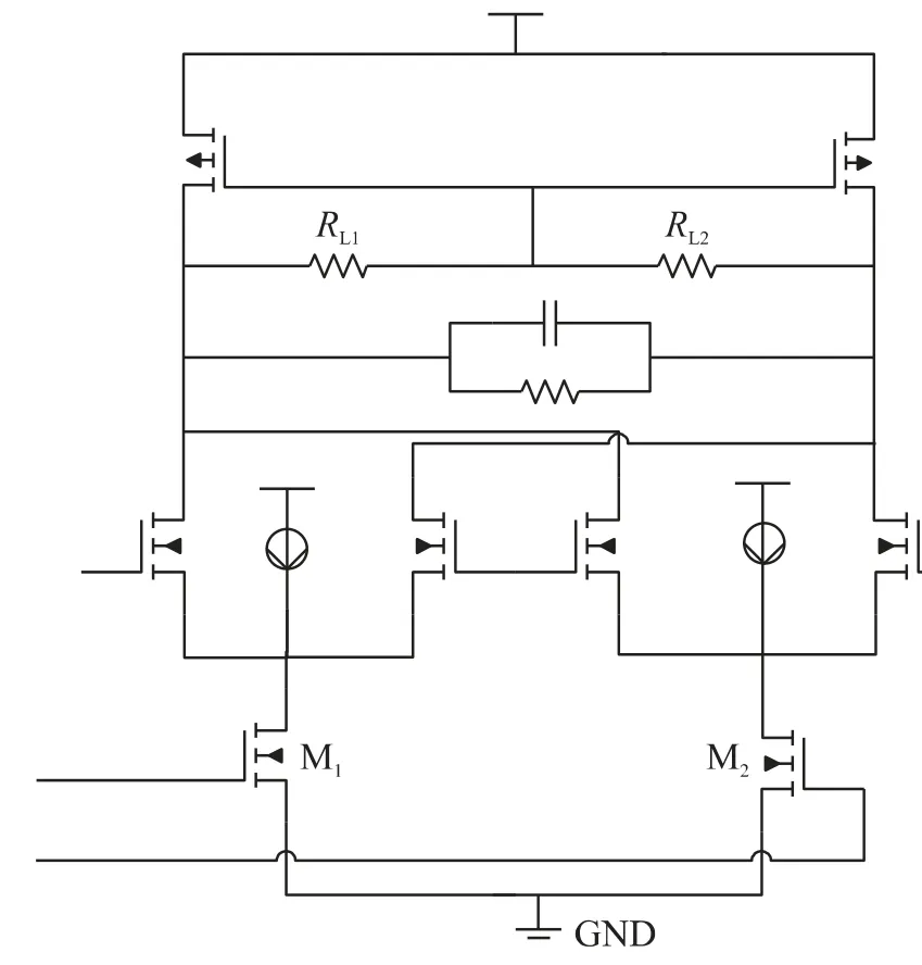
Fig.3 Schematic of Gilbert-type RF Mixer
2.2 IF Section
The mixer is followed by the poly-phase filter(PPF),as shown in Fig.4,which has three orders and is designed little differently from the conventional.In the conventional PPF,the resistor becomes larger from one stage to next stage[7].In this proposal one,the value of resistor in the middle stage is the smallest,resulting in increasing gain of the PPF with frequency.It compensates the gain of VGA,which,as we know,is always decreasing with frequency.Thus the receiver gain is kept much smoother across all of the used bandwidth.
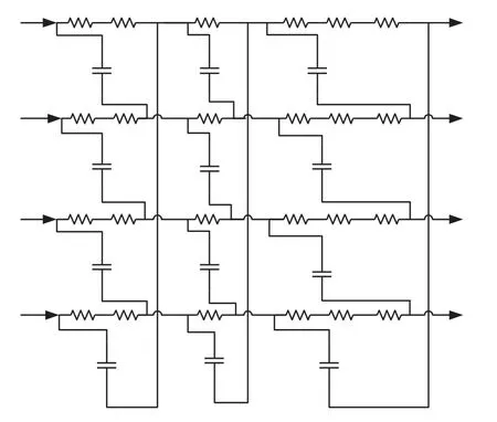
Fig.4 Schematic of the proposed poly-phase Filter
In this receiver,since the ADC is only two bits,the linearity of the IF block can be easily satisfied.Compared with the RC filter,although the linearity of Gm-C filter is moderate,it has the advantage of consuming less current;therefore the latter is used in this work,which is a six order ChebyshevⅠtype filter.
The characteristic of the filter is influenced by the output impedance of the Gm element.With the increasing output impedance,the characteristic of the filter becomes more ideal.Fig.5 shows the circuit of the filter element.This Gm element based on the simple CMOS invert was reported by Nauta[8].Compared with the conventional Gm element,which is usually implemented with cascade structure to increase the output impedance,the Gm proposed by Nauta is especially suitable for low power supply application due to its simple architecture;furthermore,it can work in very high frequency owing to the absence of internal node.The differential output impedance of the Nauta Gm element is determined by the following formula:gm5,gm6are the transconductance of Inv5 and Inv6,respectively;thus the output impedance can be very large by making gm5=gm6.

Fig.5 Schematic of the Gm-C unit

The Gm-C filter usually needs tuning circuit to compensate the variations of process and temperature.The main drawback of Nauta Gm element is the inconvenience for tuning,and the only method for tuning the Gm is to adjust the power supply,which needs a phaselocked-loop using Nauta element as the ring master oscillator[8].The oscillator and the reference signal,both with full voltage swing affect the weak signal in the analog circuit.Considering the above,no tuning circuit is implemented in Gm-C filter.We simply increase the orders of the filter to ensure the specified attenuation at the target frequency,while keeping the pass-band undiminished.
The Gm-C is followed by the various gain amplifiers(VGA),which has three stages.The gain of each stage can be tuned linearly from 0 dB to 15 dB by the AGC loop.According to the Reference[2],the duty cycle of magnitude(MAG)for 2-bits ADC output should be kept 33% in average to minimize the C/No(Carrier to noise density)due to the analog to digital conversion loss to 0.54 dB;so a charge pump-based AGC loop is proposed,which ensures the duty cycle of MAG to 33%in average by monitoring signal and adjusting the gain of the VGA.
2.3 Frequency Synthesizer
The frequency synthesizer is fully integrated,including on-chip voltage controlled oscillator(VCO),phase frequency detector(PFD),charge pump and divider,and generates I/Q signals to drive the image rejection mixer,which is implemented by means of running at twice the LO frequency and of a divide-by-two stage,implemented with ECL-like dividers.The circuit design of the frequency synthesizer is similar to those in the Reference[9-10].
The TCXO frequency employed in GPS receivers is often a multiple of 1.023 MHz,especially 16.368 MHz,which is also used as the reference frequency in this receiver.Since it is relatively high,the loop filter of the synthesizer is integrated on chip.-3 dB bandwidth is set to 150 kHz,resulting in a small RC time constant suitable for integration.A three order loop filter is implemented in the frequency synthesizer as shown in Fig.6(unclear).The parameters of the loop filter are as follows:C1=5 pF,C2=100 pF,R2=47 kΩ,C3=2 pF and R3=5 kΩ.

Fig.6 Die microphotographs of the complete CMOS receiver front-end chip occupying 2.6 mm2 die area.
3 Experimental Results
The CNSS RF receiver is implemented in a 1P6M 0.13μm CMOS process,and a die microphotograph is shown in Fig.6.The layout consumes less than 2.6 mm including the ESD protection pads.The receiver is packaged with a standard 32-pin QFN and measured with an off-chip surface-mounted-device(SMD)balun.The off chip balun used in the measurements has a typical loss of 1.5 dB,which has not been de-embedded from the results.
Fig.7 shows the phase noise characteristic of the PLL.Its phase noise is lower than 72 dBc/Hz,-83 dBc/Hz,-81 dBc/Hz,-95 dBc/Hz and-112 dBc/Hz at frequency 100 Hz,1 kHz,10 kHz,100 kHz and 1 MHz respectively,which ensure the average phase noise is below-80 dBc/Hz.Fig.8 shows a typical output spectrum at the final IF stage centered at 4.63 MHz,and the output power is about-15 dBm with-110 dBm input signal,resulting in 95 dB voltage gain.Fig.9 shows the frequency response of the entire radio.In this figure,the signal extends from 2.51 Hz to 7.8 MHz and the ripple is less than 1.5 dB with attenuation of 30 dB at 11 MHz.Due to the state-of-art power regulator design,this receiver could operate over wide voltage supply,from 1.4 V to 2.6 V,and it could run over the temperature range from-35℃to 120℃without serious performance degradation.Table 2 summarizes the measured results of the presented work.
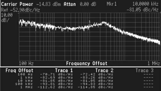
Fig.7 Measured PLL phase noise
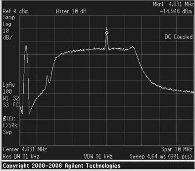
Fig.8 Measured final IF spectrum
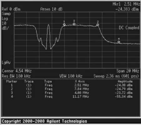
Fig.9 Measured frequency response of the entire receiver

Table 2 radio performance summary
4 Conclusion
The design and implementation of the RF receiver for CNSS is firstly presented in this paper.With the chosen 0.13μm standard CMOS technology and a few needed external components,it is designed for a complete CNSS integration in the future.Due to its low noise figure and high image rejection,this receiver provides the needed SNR for the correlation in the baseband for best in class sensitivities.The receiver consumes 28 mW from a 1.4V supply and 2.6-mm die area with noise figure of 2.2 dB.To the best of the authors'knowledge,this is the first receiver designed and reported for CNSS,while showing Competitive performance.
[1]Murphy A,Tsutsumi S,Gaussen P.A Low-Power,Low-Cost Bipolar GPS Receiver Chip[J].IEEE J.Solid-State Circuits,1997,32(4):587-591.
[2]Cloutier M,Varelas T,Cojocaru C,et al.A 4-dB NF GPS Receiver Frond-End with AGC and 2-b A/D[C]//Custom Integrated Circuits Conf.Dig.Tech.Papers,1999:205-208.
[3]Montagna G.A 35-mW 3.6-mm Fully Integrated 0.18-μm CMOS GPS Radio.IEEE J.Solid-State Circuits,2003,38(7):1163-1171.
[4]Jinho Ko,Jongmoon Kim,Kwyro Lee.A 19-mW 2.6-mm2L1/L2 Dual-Band CMOS GPS Receiver[J].IEEE J.Solid-State Circuits,2005,40(7):1414-1425.
[5]Gramegna G,Mattos P G,Losi M,et al.A 56-mW 23-mm2Single-Chip 180-nm CMOS GPS Receiver with 27.2-mW 4.1-mm2Radio[J].IEEE J.Solid-State Circuits,2006,40(3):540-551.
[6]Thomas H Lee.The Design of CMOS Radio-Frequency Integrated Circuits[M].Beijing:publishing House of Electronics Industry,2004:197-212.
[7]Farbod Behbahani,Yoji Kishigami.CMOS Mixers and Polyphase Filters for Large Image Rejection[J].IEEE J.Solid-State Circuits,2001,36(6):873-887.
[8]Bram Nauta.A CMOS Transconductance-C Filter Technique for Very High Frequencies[J].IEEE J.Solid-State Circuits,1992,27(2):142-153.
[9]Pellerano S,Levantino S,Lacaita A L.A 13.5-mW 5-GHz Frequency Synthesizer with Dynamic-Logic Frequency Divider[J].IEEE J.Solid-State Circuits,2004,39(2):378-383.
[10]Hung Chih-Ming,Kenneth K O.A Fully Integrated 1.5-V 5.5-GHz CMOS Phase-Locked Loop[J].IEEE J.Solid-State Circuits,2002,37(4):521-525.
