高增益GaN基PIN 雪崩二極管的制備及p-GaN 層載流子濃度的估算
2020-06-16 09:21:54曹子坤劉宗順江德生朱建軍陳平趙德剛
發光學報 2020年6期
關鍵詞:大學
曹子坤劉宗順江德生朱建軍陳 平趙德剛?
(1.中國科學院半導體研究所集成光電子學國家重點實驗室,北京 100083;2.中國科學院大學材料科學與光電技術學院,北京 100049; 3.中國科學院大學材料科學與光電工程中心,北京 100049)
1 Introduction
As the representative of the third-generation semiconductors,GaN materials are widely used in optical and electrical fields in recent years because of its wide band gap[1].After the two-step substrate growth technology is mature and the growth conditions of p-GaN are improved[2-3],GaN optoelectronic devices have made great progress.Compared with silicon devices,GaN based avalanche detectors have the advantages of high internal gain and fast response.The forbidden band width of the material is 3.39 eV,which can detect the ultraviolet light.It is widely used in military early warning,medical detection,electronic communication and other fields.In this paper,the fabrication and test results of a pin structure GaN based detector are introduced in detail.The p-layer carrier concentration has a great influence on the device performance.The estimation and measurement of the parameters are helpful to further optimize the device.Therefore,based on the test results of the avalanche detector,this paper proposes a method to estimate the p-layer carrier concentration.At the same time,Hall measurement and SIMS(Secondary ion mass spectroscopy)are used to verify the accuracy of the estimation results.
2 Experiments
2.1 Materials
The GaN samples are epitaxially grown on sapphire substrate by Metalorganic Chemical Vapor Deposition.Because there is a large lattice mismatch between sapphire substrate and GaN material,a thin buffer layer should be grown on sapphire substrate first.Then u-GaN,n-GaN,i-GaN and p-GaN are grown in order.u-GaN is the nucleation layer grown for reducing the lattice mismatch of subsequent growth.The i-GaN layer is unintentionally doped[4],but because of impurities,it shows weak n-type.The thickness of p,i and n layers is 0.2,0.1,1.8 μm respectively.The carrier concentration in i-layer is 3×1016cm-3and that in n-layer is 5×1018cm-3by the previous tests.The carrier concentration in player can be obtained by the subsequent calculation and tests.
2.2 Device Fabrication
In order to remove the surface contamination,the samples were cleaned with acetone and isopropanol, respectively, in a 75 ℃ water bath.Then,the inorganic impurities and the oxide layer on the surface are removed with a mixed solution of HCl and hydrogen peroxide.Both p-type and n-type contacts were then patterned and deposited using a standard lift-off process. A mesa structure was formed by Inductively coupled plasma(ICP)etching[5].The metal film is deposited by magnetron sputtering.The passivation layer is grown to reduce the leakage current through the mesa sidewalls,preventingthe devicesfrom undergoing premature breakdown under reverse bias[6].The photosensitive area of the device is about 300 μm × 300 μm.The transparent electrode is Ni/Au[7],with thickness of 15/50 nm respectively.The thickening stage adopts Ti/Al/Ti/Au[8-9]with thickness of 15/250/50/250 nm.After the process treatment,the overall structure of the device is as shown in Fig.1.
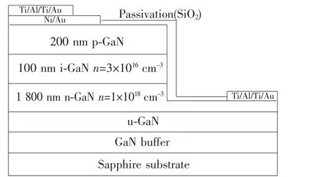
Fig.1 Structure of pin GaN avalanche detector.
3 Results and Discussion
In order to evaluate the defects of the material,the rocking curves of X-ray diffraction(XRD)are measured by Omega scanning.As shown in Fig.2,the full-widths at half-maximum(FWHMs)at the GaN(002)reflection and(102)reflection are 212.04 arcsec and 219.6 arcsec,respectively.The calculated results show that the screw dislocation density is 9.03×107cm-2and the edge dislocation density of GaN samples is 2.56×108cm-2.The above data indicate that the defect densities in the material are relatively small[10].
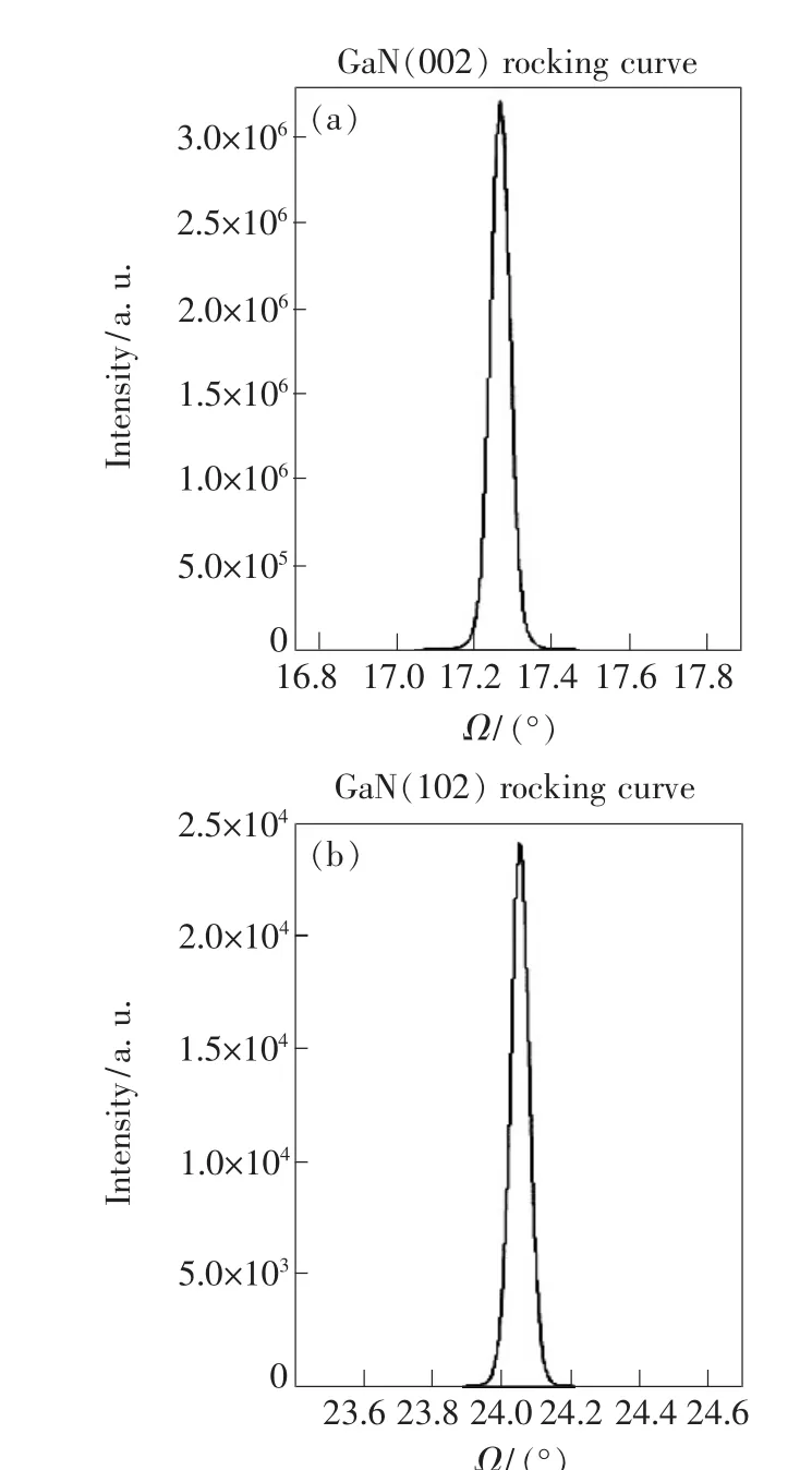
Fig.2 XRD rocking curve results.(a)At(002)reflection.(b)At(102)reflection.
The GaN material is also tested by atomic force microscopy(AFM).The result is shown in Fig.3.The scanning area is 5 μm ×5 μm.The total arithmetic average roughness(RA)and root mean square roughness(RQ)of the samples were 0.2 nm and 0.3 nm respectively.The surface morphology is flat as a whole,and the obvious step flow is also observed exhibiting excellent surface properties.
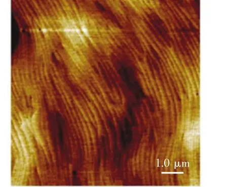
Fig.3 Measurement result of GaN surface by AFM
The I-V test device is Keithley 2400,and the current error is about 100 pA.For protecting the instrument,the maximum scanning voltage range is set to 75 V,and the voltage step is set to 0.1 V.
First,I-V curve Idarkis measured in the dark.Afterwards,using xenon lamp with 75 W power as light source,the detector area is illuminated by 360 nm band light through a scanning grating monochromator,and the I-V curve Iphotois measured.By using the equation of avalanche multiplication,the gain factor of avalanche multiplication Mphcan be determined as[11-12]
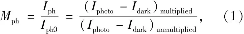
where Iph0and Idarkare the photocurrent and dark current respectively.The molecular terms of Eq.1 correspond to the current when avalanche multiplication occurs,while the denominator terms of Eq.1 correspond to the current when avalanche multiplication does not occur.Since the photocurrent of the photodiode does not significantly increase after 10 V,the unmultiplied currents are sampled at 10 V for calculating the avalance gain.The typical results are shown in Fig.4.
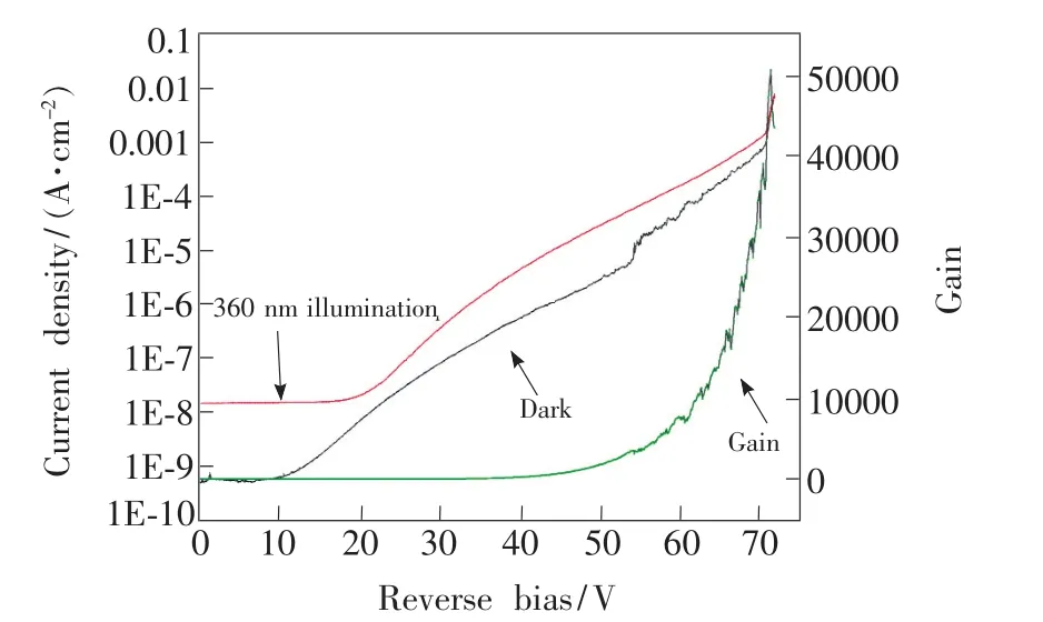
Fig.4 Typical reverse-biased I-V characteristics of a GaN APD with and without light illumination at λ=360 nm.The calculated avalanche gain is also shown.
It can be seen that under the reverse bias voltage of no more than 11 V,the current increases very slowly with the voltage,which is less than 1 nA.When the voltage reaches 71 V,avalanche breakdown occurs,and the current increases exponentially.Limited by the maximum current of the instrument, the maximum gain measured is 5 ×10⁴,which will be higher in practice.
It is assumed that the layers of GaN are uniform,and the interface charge of each layer is ignored.We use the catastrophe junction approximation and assume that there is only one kind of conductive impurity in each GaN layer.The charge distribution of pin device is roughly as shown in Fig.5.
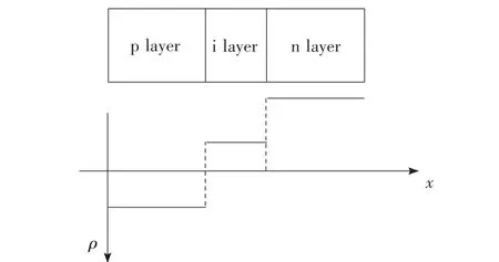
Fig.5 Approximate distribution of charge density(non proportional)
The electric field in semiconductor is affected by the charge distribution,which can be expressed as Eq.2 by Poisson equation:
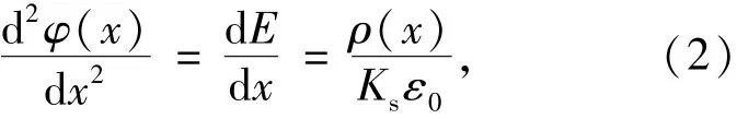
where φ is the potential, E is the electric field intensity, x is the distance, ρ is the charge density which can be approximately considered as the elementary charge e multiplying donor or acceptor concentration, Ksis the dielectric constant of GaN, and ε0is the permittivity of free space.According to Poisson equation and carrier continuity equation[13-16],the distribution of electric field intensity of the device can be drawn as Fig.6.
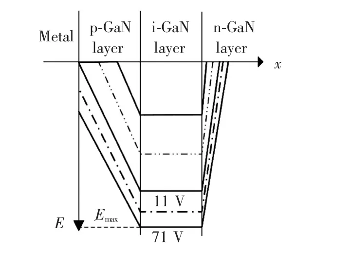
Fig.6 Electric field intensity distribution of pin device under different reverse bias voltage
It can be seen that with the increase of the reverse bias voltage,the electric field gradually diffuses to the p and n regions.Because of the high carrier concentration in n-layer and relatively low diffusion in p-layer,p-layer will be depleted earlier than n-layer.
The contact type between metal and semiconductor strongly depends on the difference of their work functions.In order to form Ohmic contact between p-type material and metal,it is generally required that the work function of metal should be larger than that of p-type semiconductor material.For p-GaN materials,the work function is about 7.5 eV[17].But the metal largest work function Pt is only 5.65 eV.In fact,the p-layer GaN will contact with the metal to form a Schottky contact with a very small potential,and then the Ohmic contact effect will be produced by using the tunneling effect under the high reference impurity.Fig.7(a)shows the conduction band diagram of pin device and metal under zero bias or low bias.At this time,the electrons in the p-layer pass through the i region to the n region,which belongs to minority carrier conduction.As shown in Fig.7(b),when the p-layer is just exhausted,the metal electrons can cross the barrier of p and i layers to the n-layer.It can be considered that the metal and the pin device are connected to form a Schottky node,and the potential height will be higher than the general Schottky node.Because the Schottky reverse current is generated by the majority carrier,while the pin junction current is generated by the minority carrier,the reverse current of Schottky junction is much larger than that of pin junction.The current generated by the majority carrier will be much greater,as shown in Fig.7(c).With the reverse voltage becoming larger,the Schottky potential is eliminated and the current becomes larger and larger.So,we can infer that when the I-V curve direction bias reaches 11 V,the current suddenly increases(shown in Fig.4),because the p-layer is just completely depleted as Fig.7(b).
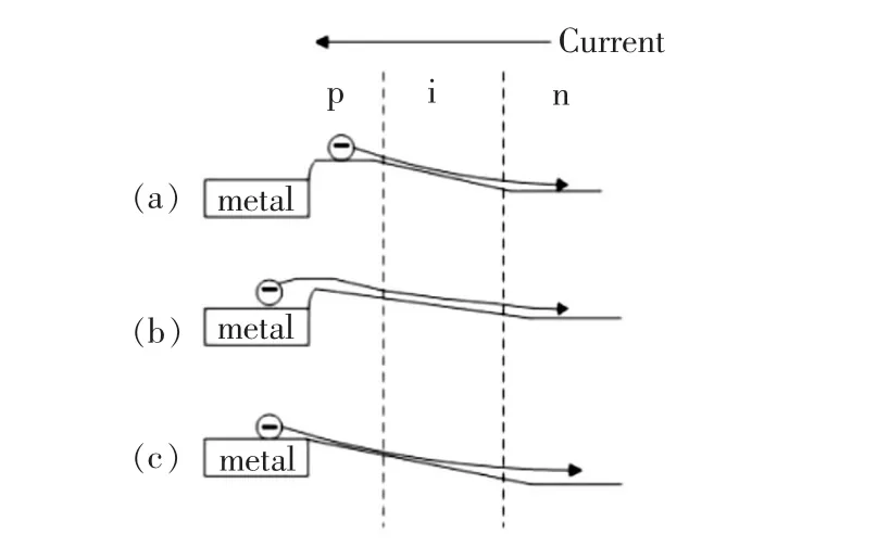
Fig.7 Conduction band diagram of pin device contacting with metal under different reverse voltage.(a)Electronic transport under low reverse voltage.(b)Electron transport when the p-layer is just depleted.(c)Carrier transport when the reverse voltage increases further.
According to the principle of integration,the area enclosed by the E-X image is approximately equal to the sum of the voltages,i.e.the magnitude of the applied reverse bias voltage VR1and the builtin potential difference Vbi.The Vviis about 3.2 V and the VR1is about 11 V when the p-layer is just exhausted.If the concentration of i and n-layer and the thickness of p and i layer are known,using the area of E-X image as the sum of reverse bias voltage and built-in potential difference,the slope of p-layer line Kpin E-X image is calculated as shown in Eq.3:
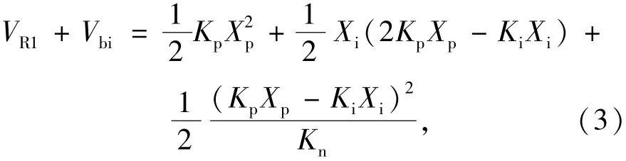
where Kp, Ki, Knare the corresponding slopes of EX images of p, i and n layers respectively, Xi, Xnare the thickness of i layer and n layer respectively.It can be calculated that Kpis 3.6×10¹⁴V/m2.Using the Poisson equation of Eq.2,the carrier concentration in the p layer can be calculated to be 1.8×1017cm-3according to the value of Kp.
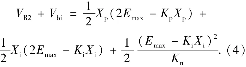
In order to further verify the accuracy of estimation methods and results.We analysis the avalanche when the reverse voltage just reaches VR271 V.When avalanche occurs,it needs high enough electric field strength inside the device to drive the carrier to collide with the lattice.However,the maximum electric field strength of the device with the same material is generally considered to be basically the same when avalanche happens.If the p-layer carrier concentration is supposed as the result of calculation above, namely 1.8 ×1017cm-3, the area enclosed by the E-X image is equal to the reverse voltage VR271 V plus the built-in voltage 3.2 V.According to the above assumptions,using the area of E-X image as the sum of reverse bias voltage VR2and built-in potential difference Vbi,the maximum electric field intensity can be calculated as 2.6 MV/cm by Eq.4 which is basically consistent with the reported value of previous studies[18-26]:
Experimental methods are also used to analyze the p-layer carrier concentration[20,27].p-GaN: Mg+layers are grown with the same growth conditions for tests.SIMS can be applied,and the concentration of Mg atoms shown in Fig.8 is about 2×1019cm-3.According to previous studies[2],1%-2% of all Mg atoms are ionized at room temperature[28].At the same time,the sample was also used for Hall test at 300 K.The average carrier concentration in the player is about 3.15×1017cm-3.These experimental results are very close to the previous estimate of 1.8 ×1017cm-3.
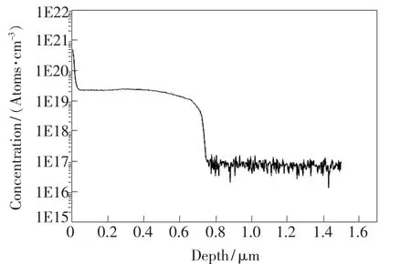
Fig.8 Secondary ion mass spectrometry(SIMS)curves of Mg atoms in p-layer samples grown under the same condition
4 Conclusion
In this work,the test results of the studied avalanche detector show that the dark current of the device is less than 1 nA when the bias voltage is less than 11 V.The gain of APD is 5×10⁴.The overall performance is quite good.The method of estimating carrier concentration in the p-layer is in line with the test results of Hall and SIMS measurements.The proposed method can be used to measure the carrier concentration in p-layer in the avalanche diode for optimizing the device design.
猜你喜歡
中學生天地(A版)(2022年6期)2022-07-14 12:39:26
大學(2021年2期)2021-06-11 01:13:48
大學(2021年2期)2021-06-11 01:13:12
海峽姐妹(2020年12期)2021-01-18 05:53:08
文苑(2020年8期)2020-09-09 09:30:16
民主與法制(2020年16期)2020-08-24 06:54:50
新世紀智能(英語備考)(2020年6期)2020-08-14 01:06:20
華人時刊(2017年13期)2017-11-09 05:39:29
浙江工業大學學報(社會科學版)(2017年3期)2017-10-13 02:23:52
中國現當代社會文化訪談錄(2016年0期)2016-09-26 08:46:07